Making a PCB - Printed Circuit Board
Prototyping a circuit onto a breadboard is a great way of testing a circuit however the resistance, capacitance and current handling capabilities can affect it's operation compared to if the components were soldered together like that on a circuit board. Making a prototype board is a step in between the large scale manufacture or for the hobbyist like me it's a flexible way to create your own boards without the hassle of using a strip-board.
There are several different methods to make a board, there are several advantages and disadvantages to each. This page will outline the most common ways to make an effective board. Ther are a couple of other methods which I have considered investing in but I simply do not have the funds to justify.
Single Sided Photo-Etch
The prototype circuit board is very simple to create and can be done in as little as 15 minutes which makes it ideal for fast prototyping work. There are some limitations however such as that the board can be a maximum of two layers, the resolution is not as accurate as a silkscreen board and there is no silkscreen for the placement of components. This method is still very common in research and development due to it's simplicity and generally great results.
The first thing you will need to do is get a design software, the one I recommend which is free is called "Express PCB". It has a small library of components but generally you will find everything you need otherwise you can place your own pins or solder tracks. It has the capability to run up to four layers, however we are only able to prototype two and even that's awkward, I would recommend staying with a single layer for now but I will show how to do two layers later.
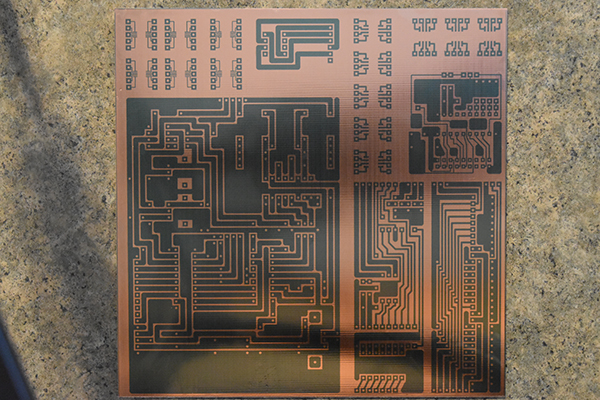
Below is an example of a board I will be creating, I'm not going to explain how to use the software because it's just that simple, if you cannot work it out then I wouldn't go any further in this venture. One thing to note is that it really does not matter what colours you choose in the software for the background and the tracks as when it comes to printing, the tracks will always be black, I would choose colours that are easy on the eyes as you may spend more time designing a board than you will realise. There is another software along with the package that allows you to draw a circuit diagram and then the pcb software will show you where the pins link, I find this irritating and choose to manually sketch a diagram and triple check the pcb design afterwards.
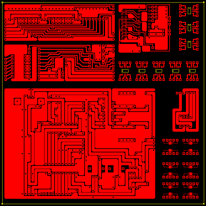
One thing you will notice when it comes to printing your design is that it is placed in the middle of the page, which is a little wasteful. Don't bother trying to resize your board in the software as the maximum is 6" by 8", any bigger and it will scale down the design. I originally used to print screen it into paint, then into word, scale and print to get a bigger design, this is however a very time consuming method. If your making boards any bigger than this then I would recommend using a different software, most of the free ones will not cut it, there are some low-cost solutions, always check the reviews before purchasing one to get the best deal. Print out your design and measure the pin spacing with a ruler, if it has down-scaled then you will have to make the board layout smaller, this is just a test so you can discard this printout.
Next you need to choose a method of how your going to develop your board, one is to use the "ironing" method or the other is to use the "photo-etch" method. The ironing method is to simply print out your design with a laser printer on a piece of paper setting the DPI printer setting to it's maximum, you then iron the design to copper clad board, after several minutes you wash off the paper with warm water and your design is stuck to the board. The main issue with this method is that you need lots of heat to get the toner to stick to the board, this will warp the board (toner is basically plastic). I used to use this method as a cheap alternative but I found it very difficult to get all of my design on the board, I do not recommend this method at all. You will find in the long run it will cost you more in scrapped pieces of copper clad board.
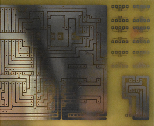
The second method is to "photo-etch" which requires a special positive sensitised clad board, it is slightly more expensive but it's really the only method to produce excellent results. The design should be printed on a clear film, tracing paper may work and wetting regular paper may also work, clear film would be the best choice. Clear film should be printed with a laser printer but some people have had great results with inkjet too, although laser printers are so much cheaper in the long run. Now you have the film such as that of the one below, make sure the blacks are strong and the lines are sharp. I chose to scan this film to post it on here, if your scan is black then your ok, if it's grey then you need to increase the DPI setting on your printer.
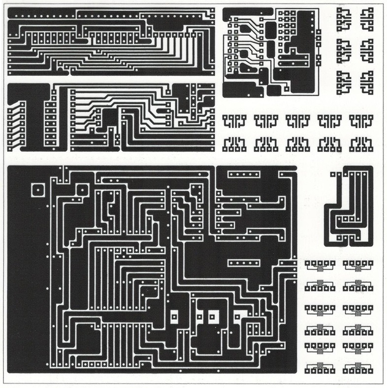
One thing you may notice with the design software is that the detail is only apparent when you zoom in really close or choose to print the design.
If you compare my screen shot to the printed layout to the left you can see the detail is much different.
Choosing to print screen the design and piece it together to make a larger design in paint would be very time consuming due to the clarity only becoming clear with a very close zoom.
It is better to upgrade software package if you require boards bigger than 6 x 8".
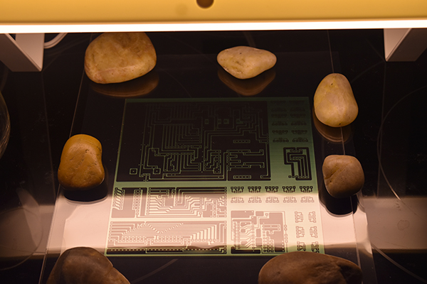
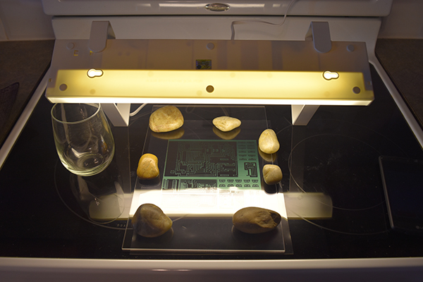
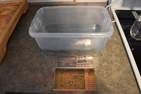
The next thing you will need is an exposure light, a daylight fluorescent is what you need, you do not want black light / UV. You will also need a piece transparent plastic the size of your film. The clad board needs to be removed from the packet, the film removed and placed photo side up. Place the film over the board (printed side down) and then the plastic sheet on top, you need the film to be perfectly flat against the board otherwise you will have detail issues later on. Switch on the light and leave for 2 minutes, then change the position for another 2 minutes, a total of 10 minutes. Moving the light in different spots will ensure that the board gets an even coverage, if you don't do this then you will have etching issues later.
After exposure you need to develop the board immediately, this is the most critical step and will make or break the etch process. The section of the board that was hit by the light needs to be removed, this requires sodium hydroxide / caustic soda. This stuff is acid, wear gloves and eye protection. You can make up your own solution but will get more accurate results buying some specifically designed for pcb developing as the concentration will be accurate along with the time given, it is normally watered down 10:1. Pour the solution in a plastic or glass tray, place in the board and lightly brush it with a sponge, after between 15 seconds to 1 minute you will see the developer remove, soon as it's all gone you need to remove the board and wash it, any longer and you may risk removing all of the developer. There is a silicate based developer that's supposed to be less harsh and very difficult to over-develop the board, I have not used it so cannot comment.
After the board has received a good rinse it is now time to etch the board, note you should not scrub the board. The etch will dissolve all of the exposed copper, the best stuff to use is ferric chloride as it has the fastest etch time and longest shelf life. Some other stuff to use is ammonium persulphate, it's clear and will not stain like ferric chloride will however it has a short shelf like of three weeks. The hotter ferric chloride is the faster it will etch, at 45 deg C it will etch a board in five minutes, at 20 deg C more like twenty minutes. The solution needs to be agitated basically refreshing the solution above the clad as it will etch very slowly otherwise. To agitate the solution it is best to place the board upwards in a tank and use an aquarium air pump to bubble air past the board, this keeps the solution moving. A tank heater can be used to heat the solution to no more than 45 deg C however it will fume and then must be done outside in or in a ventilated area.
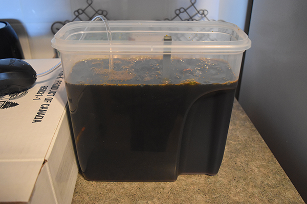
I prefer to let the solution adjust to room temperature as etching will still be only 20 minutes and theres less chance of over-etching, this is when copper etches under the tracks severly thinning them.
I then check the board after ten minutes, rotate it and then again in another 10 minutes. The other option is to rotate it every 5 minutes by 90 degrees, this ensure even etching.
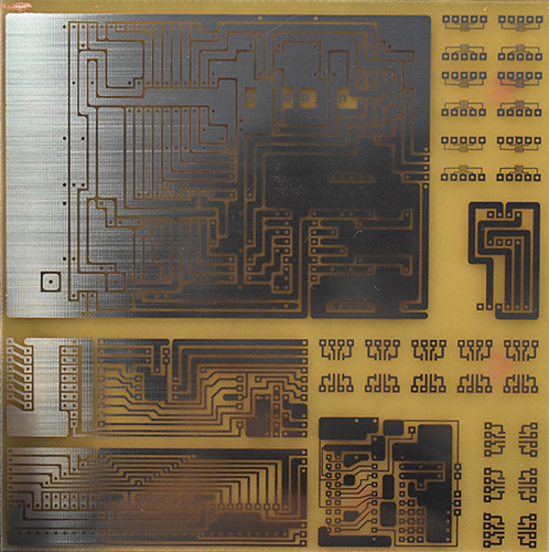
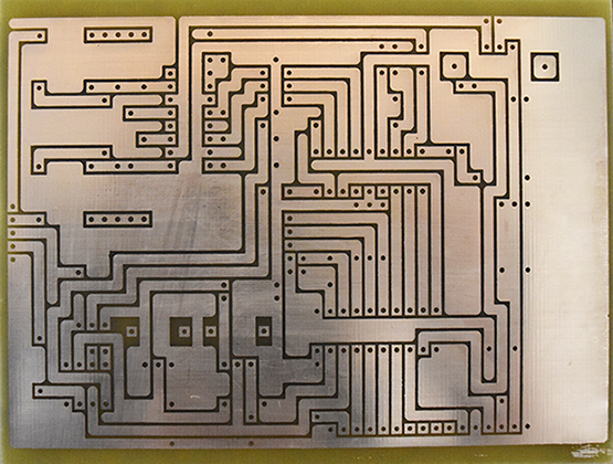
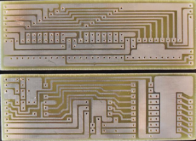
After all of the copper has been removed you need to thoroughly wash the board in soapy water, wear gloves as ferric chloride will stain everything and attack most metal including your sink. Below is the board after etching.
It is quite surprising the amount of detail you can get with this etching method, for example to the right is a surface mount adapter for the u10Max package, the chip is only 0.08inch wide.
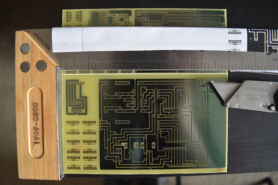
Cutting the board can be a pain in the butt, using tin snips will shatter copper clad board but since positive board is phenolic then you may be ok. The best method is to use a shear but these can be expensive, if your making a lot of boards then it is a must. I however don't make many boards so I choose to use a ruler and utility knife. I score the board several times on both the top and bottom, place the line in a vice (or a set of drawers in my case) and simply snap the board. The board always breaks cleanly due to it being phenolic, I clean the edges with glass paper.
The board datasheet says the developer does not need to removed and that soldering will burn it away, it will but you may require a little more heat. You can easily remove the developer with rubbing alcohol and then solder the board or you can tin plate it. Cold tin plating solution is readily available at most electronic hobby stores, all you need to do it thoroughly clean the board with alcohol, place the board in the solution, wait ten minute and the board is plated. Tin plating will help improve soldering (especially on surface mount) and stop the copper layer from oxidising, a lot will say it's unnecessary, it can be if your soldering immediately after removing the developer, I choose to tin plate simply because I have the solution at hand.

Drilling the board can be done will little cost by using either a small pillar drill or a dremel. A pillar drill will yield the most accurate results, it's not exactly compact but will do the job great. I choose to do it by hand with a dremel, you can also buy a pillar for the dremel. The drill bits to use should be HHS, you can bend and sharpen them, they are robust. I would not recommend carbide as these break really easy, they also have a different point geometry which unless you clamp your board down will ensure you will break the bit. The drilling speed needs to be fairly slow for the best control, the slowest a dremel can go, I have a 120Vac single speed one at over 30,000 rpm, since the motor has brushes I connect the plug to a DC supply, at 40 to 50V the dremel drills at the best speed. I had to sharpen my drill bit after just two of these boards, phenolic really blunts the bits fast, running a higher drill speed will also dramatically reduce drill life.
All of the holes should be drilled at around 0.8mm, for headers and transistors 1 to 1.2mm, you can always drill a hole bigger, the tighter the component fits the easier it makes soldering. Soldering feels like the most rewarding process as you see your board nearing completion. A big mistake with soldering is heat, 20W or 360 deg C ( 700F) is all you will need for PCB components. Clean the tip of the iron with dry kitchen roll, it will burn but will not damage your tip, the wetted sponge with thermally shock the tip making it brittle. Don't hold the tip on the track any longer than necessary, you may damage the component and the board. Press the iron tip between the component leg and track, melt a tiny amount of solder between, hold the iron until it pools and remove it.

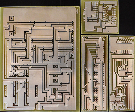
Creating a prototype board is a fairly easy and satisfying process, the board manufacture itself can be done in as little as 15 minutes and the whole process in maybe an hour. Of course these boards are nothing like what you will find in modern equipment but you may still find boards like these in older electronics as everything used this process back them. There are many companies out there that will do multiple layer boards with professional results at little cost but lead times can be long. Once you have the equipment to make your own boards you only need to pay for the copper clad as the ferric solution will last a long time, the less copper you etch the longer it will last, board design is also a crucial component to keeping costs down.
Double Sided Photo-Etch
Under Construction
Single Sided Engraved
Under Construction
Double Sided Engraved
Under Construction
A Comparison
Here is a table with a comparison to how effective each of these solutions is to make a board.
Under Construction
Hello, if you have enjoyed reading this project, have taken an interest in another or want me to progress one further then please consider donating or even sponsoring a small amount every month, for more information on why you may like to help me out then follow the sponsor link to the left. Otherwise you can donate any amount with the link below, thank you!