Microcontrollers 15 - Serial Peripheral Interface
SPI is the single most common serial interface that you will use because there is such a high flexibility with regard to it's speed and easy of use. The key difference with SPI is the number of pins it will use as there is one for data out, data in, clock and chip select. It means that when choosing SPI you will need to consider the amount of pins available on a chip and the amount of serial devices you wish to control. The data lines and the clock are shared between devices, it is the chip select pin that enables that device, therefore you require a chip select pin for each additional external device.
There are two modes in which SPI can run; Master or Slave
The master chip is generally the microcontroller, this is what generates the clock pulses. The slave is the external device such as EEPROM, ADC, SRAM, etc... I will always be choosing to run my chip in master mode.
Firstly you must find a microcontroller that supports the SPI function, it will likely be called the MSSP (Master Synchronous Serial Port) in the datasheet. Since the 16F628A does not support this I will be going with the 16F690, it has a similar footprint to the 16F628A but has all the capabilities such as MSSP and ADC as the 16F887.
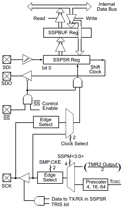
To the left is the flow diagram of how the SPI system works in the microcontroller, one thing to note is that it is double buffered which means it can simultaneously send and receive, one register deals with the port and the other holds the data.
First of all the "SSPBUF" is the register that we can access, so if you want to transmit data then you place it in there or if you receive data then you must pull it from there. The "SSPSR" register is not read / writeable, this is loaded with the data to transmit from "SSPBUF", as it transmits the data it is filled up with the incoming data, the incoming data is moved to "SSPBUF". With the USART you could transmit / receive independently as they both has two separate registers, with these registers that has to be done more carefully. Data can be transmitted out of the "SSPSR" register at the same time it is being received into the register however this cannot be continuous as the "SSPBUF" can only hold one word at a time.
The "SS" pin is known as the slave select pin, so if I were to set the microcontroller as a slave an external chip could enable it's "SSPSR" register when it wants to communicate with this particular chip. Since this will be the master I will have to designate a pin to control the slave select on the external chip, such as an SRAM chip.
The clock has many functions and this is where most of the room in the control registers is taken up. The clock select will determine whether the clock is positive or negative at idle, it also determines whether the clock is internal or external depending whether slave or master mode has been chosen
SMP and CKE are to control whether data is clocked on the rising or falling edge and whether data is inputted in the middle or the end of a clock.
SSPM is to control the clock source and what kind of prescaler it will have. Generally the clock source will be chosen to be internal at the fastest speed the external devices can operate at. It also controls whether the chip is in slave or master mode and whether we are running SPI or I2C.
There are two control registers and a status register associated with the MSSP, one of them is solely used for I2C and will be discussed in the next chapter. I will first discuss the control register as this only needs to be setup once, the "SSPCON" register. It does however have two indication bits, one is for I2C master and the other only concerns slave mode, these can be ignored.
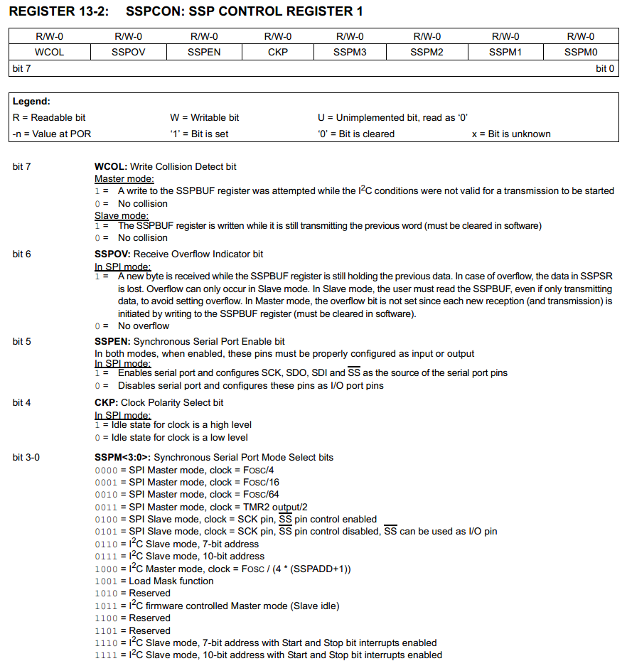
WCOL - This is no concern to SPI unless it is in slave mode, with proper programming this should never flag.
SSPOV - This will flag when more incoming data has been received when there is no room for it, SSPBUF has to be read before receiving more data.
SSPEN - This will enable the serial port, unlike the USART port the inputs and outputs have to be set to their function (not all to inputs like the USART).
CKP - Clock polarity at idle almost always wants to be low, therefore set to zero. This may be changed if your using a transistor on the output and wish to invert the signal.
SSPM - This will select between I2C, SPI and where we want our clock signal to come from. I would normally choose to clear all of these bits or set bit 0 for a quarter slower operating speed.
The status register will require you to read it to see if data has been received, below is the "SSPSTAT" register. Since most of this register is associated with I2C I chose to delete it out.
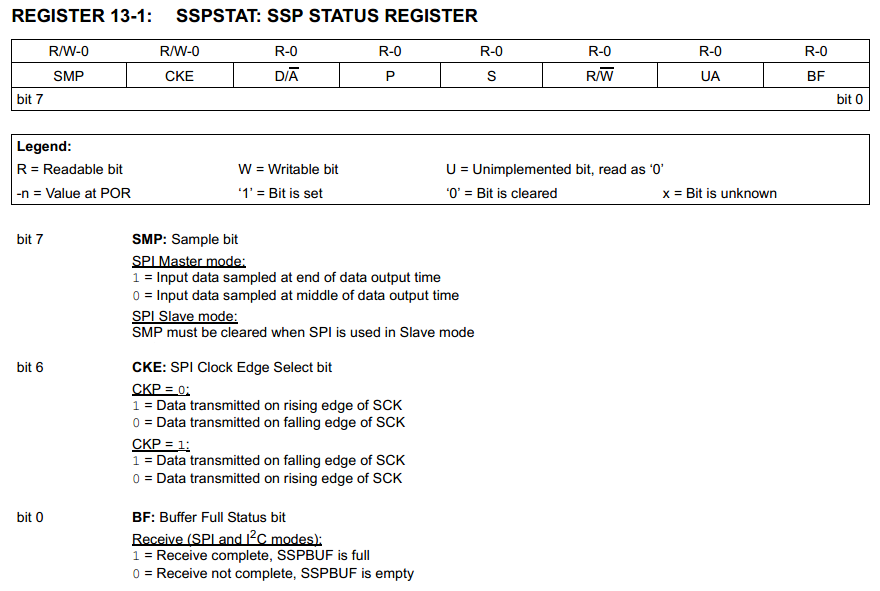
SMP - The data in almost all instances will be sampled in the middle of the data.
CKE - In general data is always transmitted on the falling edge of a clock signal. This bit is to be set.
BF - This will indicate when data has been received.
There is very little needed to setup the SPI function, it is actually the easiest serial function to deal with. Anything placed into the "SSPBUF" will be transmitted, anything to be received is placed into "SSPBUF". To receive information quite simply the "SSPBUF" register has to be written to, the "SSPBUF" data will be replaced by the received data and the "BF" bit will flag. To clear the flag the "SSPBUF" register has to be read, to receive more data it has to be written to again. The slave device may not have an input and therefore the transmitted data will be ignored. If the output pin is not in use then it can be configured as an input pin to be used normally, likewise if the input pin is not used then it can be configured to an output an used normally.
In the previous chapter I mentioned a type of memory called FRAM (Ferroelectric Random Access Memory) as a faster and longer working life non-volatile memory alternative to EEPROM. I will also be talking about SRAM (Static Random Access Memory) which is also a fast alternative to a large expansion of RAM since internal is limited to around 256 bytes in most microcontrollers. The SRAM chip is known as the "23LC512" which has a storage area of 512kbit, the FRAM chip is known as the "MB85RS64B" which has a storage area of 64kbit. Both of the chips can accept a clock rate of 20MHz which is a far faster capability than the microcontrollers 5MHz clock output.
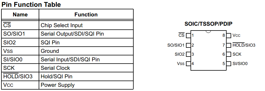
Here is an example of the pin diagram for the 23CL512.
The pins with a bar above them are inverted meaning that to use this function they must be pulled low.
All unused pins should be pulled high via a resistor, HOLD and SIO2 are examples of unused pins.
The difference with the FRAM chip is that pin 3 has a different function, it is a write protect pin that is pulled high for normal operation. You will notice that for 8-pin SPI memory chips that the layouts tend to be the same, pin 3 will normally be a special function pin. The hold pin is used to pause the chip, this may be if another chip has to be selected part way through a transmission, it is like an interrupt, when the hold is released it can resume transmission, hold is generally not used and pulled high for normal operation. The great thing with SPI is that it's a standard and with a standard comes a universal protocol and instruction list. Below are the instruction lists from both chips.
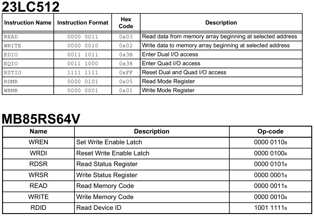
You should notice that instructions such as read / write and the status read / write have the same instructions for both chips. There are however a few additional instructions in both of the devices. The 23LC512 has instructions to enter "dual" or "quad" IO mode and an instruction to reset this mode. These modes allow the user to use additional I/O pins for data transfer splitting the information equally across them. For example if you were to send 8 bits down a single line then you would send 4 bits each down dual lines and 2 bits each down four lines. This will greatly increase the data transfer however most microcontrollers will not support this feature unless you choose to "bit bang" the information, and since bit banging is slower you would be better with using the SPI register with a single data line. On the second device you can enable / disable the write and read it's ID, with this FRAM chip you must send the enable write latch every time you want to write as when write is completed the latch will reset itself.
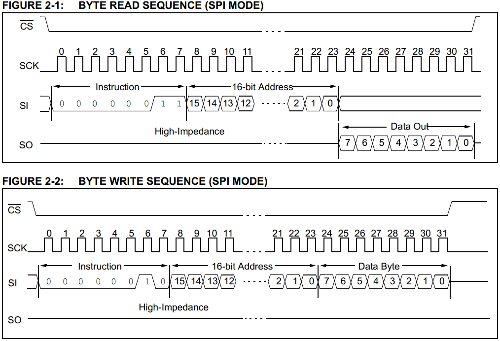
As for the data, as mentioned earlier the chip will only work if it is selected, this is the "CS" pin which is pulled low in order to select the chip, if left high the device will ignore all incoming data. Firstly the instruction is sent followed by a 16-bit address and then either the data in or out until the chip has been deselected. All SPI devices will accept an 8-bit instruction, a 16-bit address and then input / output 8 bit data, the difference between some devices is they may only deal with one word or many. For the SRAM chip it will input / output a 32 word page and continue to loop on itself until the chip has been deselected. The FRAM chip will continue to increment it's address even when the address counter rolls over, you can fill the contents a lot faster than the SRAM.
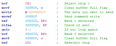
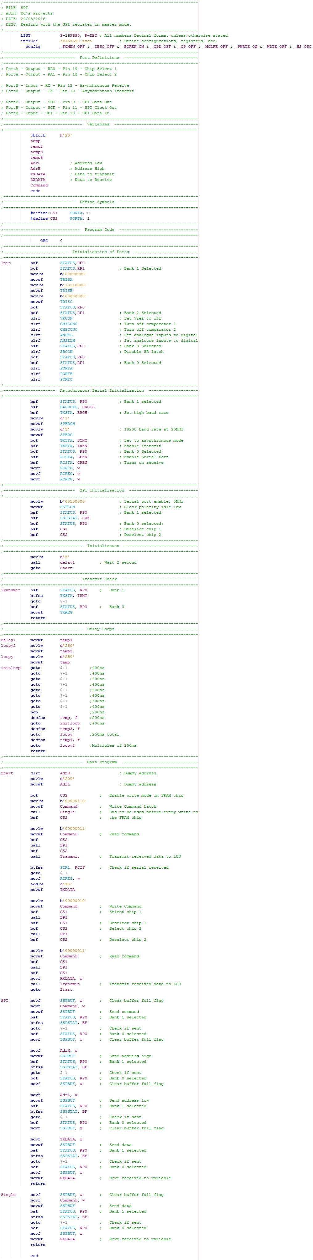
The small section of program below is what is required to read or write SPI, note that reading and writing happen at the same time so this code is universal. Firstly the chip is selected by outputting a pin to low, this pin will connect to the external chip telling it to be ready to receive / transmit (normally the pin is labeled as SS or CS). A bit will flag if the buffer contains information, to remove this flag the register must be read, this buffer should always be emptied by the previous serial command. The data to be transmitted is placed into the buffer which immediately causes it to send the information and replace the buffer with the received information. When this has completed the buffer flag bit will raise indicating the buffer is full, the program will branch. To be able to send / receive more data the buffer flag must be cleared otherwise it will cause an overflow condition and stop the SPI module. To clear the flag the contents of the buffer must be read, the contents can either be used or discarded. The chip is deselected to tell the external chip it has finished communicating.
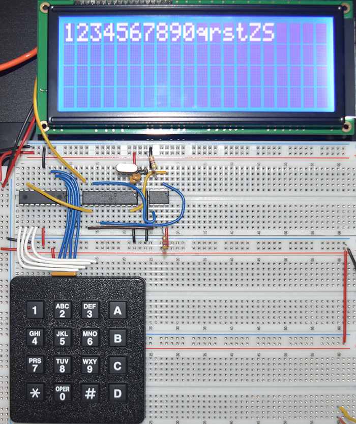
For the main program all it will do is read an input from a serial keypad, the data will be saved to the SRAM chip, it will then be loaded from the SRAM to be displayed on an LCD. I'm just creating a simple program to show how easy it is to interface with an external SPI device. As you will see in the following program the initialisation of SPI is a lot easier to setup than asynchronous, infact it is a lot faster with almost no chance of error.

By connecting the oscilloscope to the microcontrollers clock and data output you can see the speed at which serial can operate.
This is the fastest SPI can be run on this particular microcontroller, the gaps between the transmissions of data cannot be reduced due to the buffer flag requiring to be checked.
A total of eight words in as little as 25us will still yield a bit rate of 2.56Mbit/s which is pretty fast compared to all other forms of serial.
Just sending one word is infact a speed of 5Mbit/s.

Another difference with SPI compared to other forms of serial, especially I2C (explained in next chapter) is the speed at which the inputs can charge.
A lot of serial devices use what is known as an "open drain" which can only pull current down meaning that it requires a pull up resistor, the smaller the resistor the faster the device can run however the more current it consumes.
The difference with SPI is that it uses CMOS which is a push-pull device, it is able to sink and source current meaning it can switch at a much faster speed.
In slave mode this chip is supposed to be able to handle a speed of up to 10Mbit/s.
Serial is a very fast and simple method which helps to reduce the footprint required.
This little 8-pin chip alone can hold 250 times the SRAM than the microcontroller.
The next chip to connect to this setup is the FRAM chip which will hold 31 times more non-volatile memory than the microcontroller while being able to run at 3125 times the speed of the EEPROM, and a million times the write endurance. EEPROM now seems to have little use in the modern world.
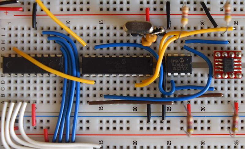
Quite simply all that needs to be changed to add an additional chip is the use an extra chip select pin, the data in, out and clock are all tied together. Below is the extra footprint on the breadboard.
Below is the revised program to accommodate the additional chip. The program will read the data from the keypad and send it to both the SRAM and the FRAM, it cannot be done simultaneously due to their outputs as they may clash. The value is retrieved from the SRAM and displayed on the LCD. When the power is cut and the chip started up again it reads the contents of the FRAM and displays it on the LCD, this proves that the FRAM chip is retaining it's memory.
Since the protocol of SPI is the same for all of the devices it meant that I could greatly reduce the size of the program since both the transmit and receive happen at the same time.
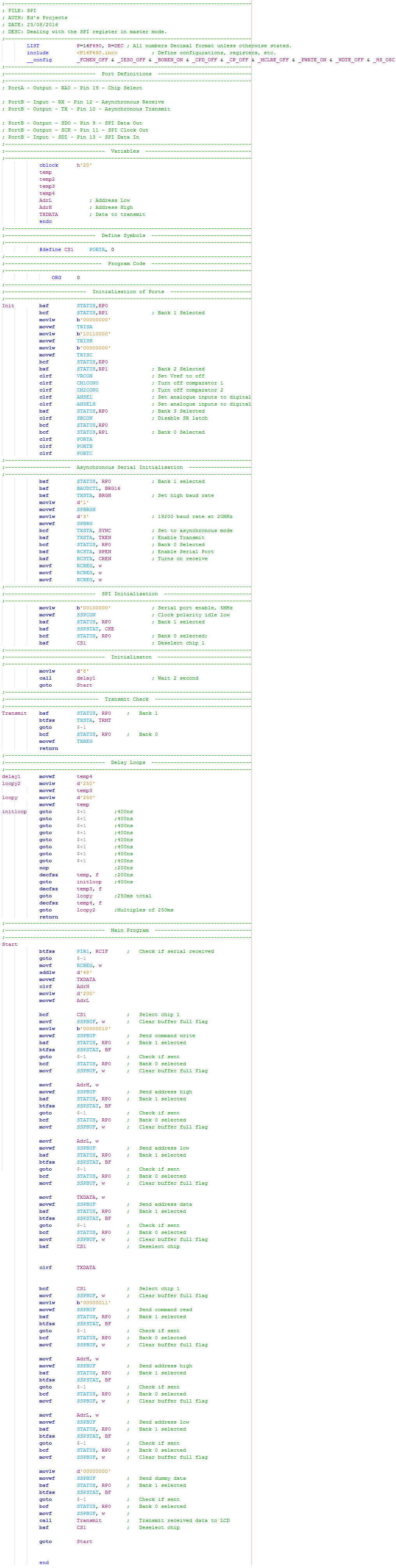
Here is a link to the - Program
As you can see SPI is probably one of the best and fastest methods for dealing with data transfer, for most applications this also provides the single most reliable method for transmitting data. This chapter has also proven why the use of EEPROM is simply not needed due to it's short write life and long write cycle. Again it all depends on the application your needing external memory or other devices for but in general asynchronous is old technology and generally used when a low pin count needs to be used or where speed is of little concern such as for an LCD or keypad. SPI is great for very fast communication, applications where you can't be waiting for the next byte of data to be sent / received, it does however require a larger pin count. Now there is one other method of serial communication known as I2C, it combines both the SPI's speed and asynchronous's low pin count, it is discussed in the following chapter.
Hello, if you have enjoyed reading this project, have taken an interest in another or want me to progress one further then please consider donating or even sponsoring a small amount every month, for more information on why you may like to help me out then follow the sponsor link to the left. Otherwise you can donate any amount with the link below, thank you!