Microcontrollers 9 - 16F887
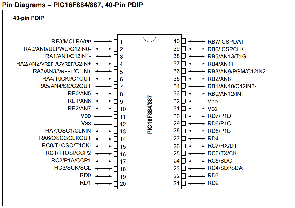
I had already used all of the available pins on the 16F628A and now it is time to go onto a larger chip, the 16F887, this chip will now be used for most of the future projects. This chip has 34 inputs / outputs I can use with an external crystal, the program memory is about 8k and there are 14 possible analogue inputs. It must be noted that the 16F887 is newer than the 16F887A, if you choose the "A" version then you will likely encounter some problems with my code.
Firstly the special configuration settings, now because this chip is also a newer model than the 16F628A it has some extra configuration settings. I have included a brief description of what they all mean, you can also set the config as a 15 bit binary number / word but symbols are so much easier to work with.
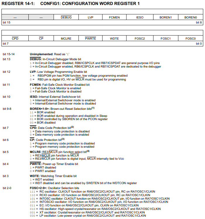
DEBUG - A debugger is something that can analyse a program for you to check for problems. So this option could allow you to externally start, stop, step through the program while it is imbedded in a circuit. It can also allow you to look through registers, RAM and EEPROM.
LVP - Low voltage programming - The same pin that is used for programming can also be used as an input, running in this mode with an input at that pin will put the chip into program mode and make it do silly things. When disabled the chip is programmed in HVP, high voltage mode, the MCLR pin is set to 9V which will reset the chip and place it into a programming mode.
FCMEN - Fail-safe clock monitor - If the external clock was to fail then the internal clock would take over, it's extremely unlikely for a crystal to fail.
IESO - Internal / External switchover bit - This can allow the chip to swap between oscillators, a slow speed for power saving or a high speed for calculations.
BOREN - Brown out reset - When the supply drops below a certain threshold it will hold the chip in reset until the supply is sufficient enough, it is useful in preventing strange activity in a chip if there is a voltage drop. It does however consume extra power, so may be disabled in battery applications.
CPD - Data code protection - The EEPROM is protected and cannot be externally written, only in the program itself.
CP - Flash program memory code protection - this is the main code that is protected, if enabled it cannot be read by hardware, for example it will stop a third party from stealing your code.
MCLRE - External master reset - This pin can also be used as an input pin, it is worth disabling the reset to get this extra capability unless a reset is needed.
PWRTE - Power up timer - This keeps the chip held in reset for 72ms to allow the supply voltage to rise to a suitable level when powered up, it is normally used in conjunction with the brown out reset as this will then hold reset for the supply to reach a certain threshold and then hold an additional 72ms for the supply to stabilise.
WDTE - Watchdog timer - This is a timed reset and a counter. The timer counts up to 18ms and then resets the chip, if a command called "CLRWDT" is instructed then the timer begins again, this is to prevent a chip from getting stuck in a loop. The 18ms delay can be prescaled up to 128 times, around 2.3s maximum in time. This is rarely enabled, a good program should never get stuck in a loop.
FOSC0, FOSC1, FOSC2 - This is to set the chip clock frequency, there are options for internal and external, I will show an example later.
As I explained in an earlier chapter there are sometimes two configuration bytes, it is quite normal to leave this one out as it's not all that important.
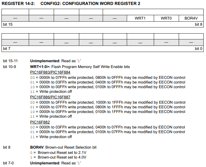
WRT - Memory self write - This can allow you to write program memory to the chip while it's running, not something I have ever done. It is done with almost the same code when writing EEPROM.
BOR4V - Brown-out reset 4V or 2.1V - This is just an extension of the brown-out reset, this is the threshold voltage for the reset to be unclamped.
Personally I wouldn't ever bother with config2 as the software will choose its own defaults.
Below is an example of the code with all of the configuration 1 symbols listed. Since there are two configuration registers you must label them like I have done, you must also write them in capitals as the software will not recognise them. As a general rule all of the mapping registers are capitals and all of the labels, instructions, variables and comments tend to be lower case.

Something I never explained was the chip initialisation, not only where you set the pins as inputs or outputs but other settings such as the analogue inputs and the comparator inputs. The problem with a lot of chips for first time users is that they can get some unusual behaviour from the chip if the ports have not been configured properly. For example some of the pins can be used as analogue inputs, infact the 16F628A chip was already configured for analogue inputs as it's default and this had to be switched off to use the pin correctly, I'm talking about the comparators. I'm not sure what the defaults are on the 16F887 but it is good practice to make sure they are switched off.
I will deal with analogue inputs and comparators in a later project but first we must know what to look for in the datasheet in order to turn all of them off. There are two sections in the datasheet that are specifically for each of these functions, there are normally two registers associated with the function, one for configuration and the other is normally the input/output. So for example the comparator configuration is as follows;
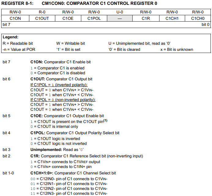
There are quite a few options to choose from, the ones to look for are the enable/disable functions. It seems that if bit 7 is set to logic 0 then the comparator is disabled. There are two options with setting this byte, either just bit 7 can be cleared or the whole register can be cleared as we are disabling it's whole function.
Since there are two comparators on the chip there will be two registers to configure, in the next case "CM2CON0".
It's not very often that a comparator will be needed and if one is it's common to use an external one instead.
You will notice that when searching through the comparator section of the datasheet you will come across quite a few different registers, one to watch out for is "VRCON". This is a voltage reference which is connected to RA2, this also needs to be disabled. Bit 7 enables the Vref and bit 6 connects it to the pin RA2, therefore both of these must be disabled, all the rest of the functions don't apply when it's disabled so I can just clear the whole register.
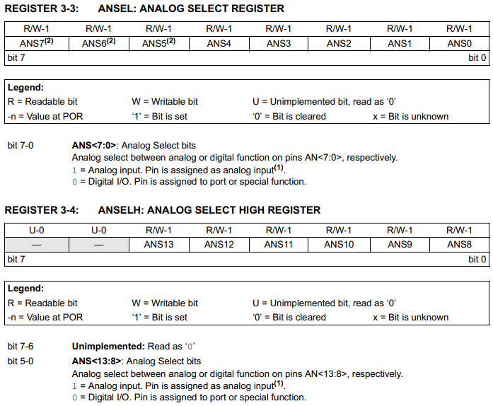
The next step is the ADC (Analogue Digital Converter) register, there are two separate registers, the port control registers and the ADC control registers. The port control registers define whether the pin is to be an input or an ADC input.
Both of the registers "ANSEL" and "ANSELH" need to be cleared to set all of the inputs as digital inputs.
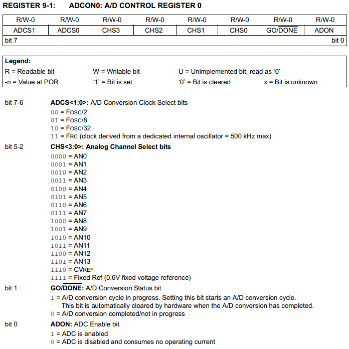
There will be two control registers and two output registers. The first control register is to the left, for now all I need to do is disable this function, since I'm doing that I can clear the whole register.
It is not really that necessary to clear the "ADCON0" register as clearing the "ANSEL" and "ANSELH" registers has already disconnected these pins.
The second control register has further options with regard to pin control, this can be ignored for now.
There are two output registers because the ADC function works in 10-bit and therefore must be split into two registers.
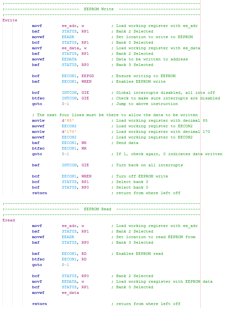
Another concern is when dealing with EEPROM as there is now an additional two registers, the special function registers are also placed in different banks so care must be taken. Below is an extract from the datasheet showing these additional registers. Both of them are high registers and extend the data register from 8-bit to 14-bit and the address register from 8-bit to 13-bit. Now in this chip there is still only a maximum of 256 bytes of EEPROM data, so why the extra bits. Each instruction consists of a 14-bit word, each address in program memory is a 13-bit word, there is also an extra bit in the control register that allows data to be written to the flash program memory and this is why the extension is needed to these registers, it really has very little to do with the EEPROM.
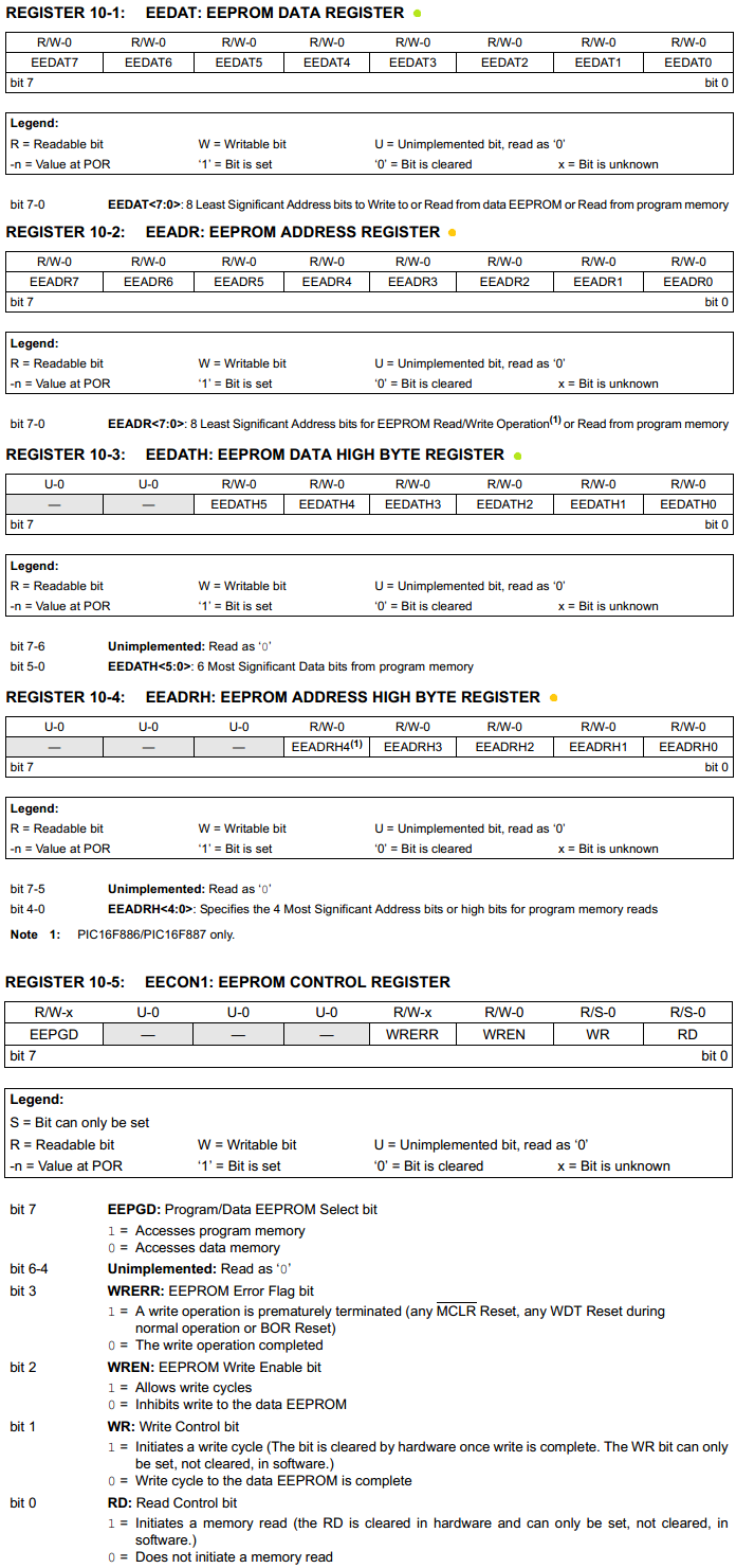
Firstly there are a total of six registers associated with the EEPROM read / write, five of those shown in the image to the left.
EEADR - These the least significant bits of the address where the EEPROM will be stored.
EEADRH - These are the most significant bits of the address where the data will be stored in the program memory. This register is of no concern with regards to EEPROM as the memory is only 256 bytes. It becomes useful for writing flash memory, this topic will not be covered in this chapter.
EEDAT - These are the least significant bits of the data which is to be sent to the chosen EEPROM address.
EEDATH - These are the most significant bits of the data which is to be sent to the chosen memory address, allows 14-bit data to be saved in program memory, for example an instruction.
Compared to the 16F628A the 16F887 has an additional control bit.
EEPGD - This is to select whether your dealing with the flash memory - the program itself or the EEPROM memory. Since I will never deal with the program memory it is quite advisable to set this bit to zero in the initialisation stage of the program and leave it zero.
WRERR - This is if the chip has been reset while the EEPROM is in the process of being written, the bit will flag as logic 1. Normally this bit can be completely ignored.
WREN - When logic 1 this will allow data to be written to the EEPROM.
WR - When set to logic 1 this bit will initiate the write sequence of the data to the EEPROM, when the process has been completed this bit will set itself back to 0.
RD - When set to logic 1 it will read the selected EEPROM address register and place it in the EEDAT and EEDATH registers.
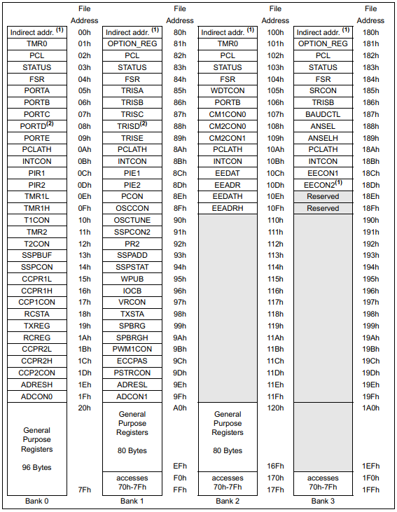
Here are the mapping registers for the 16F887.
As you can see most of the registers in the 16F887 are in the same place as the 16F628A where others are not so it is worth looking in the datasheet, otherwise if there is no access to a datasheet then the "banksel" command can be used.
There is quite an addition to the number of special file registers and I will try to cover most of these in future chapters or projects. The ones I will be concentrating on in the next few chapters are those that deal with timing, analogue, serial and interrupts.
A notable change is the location of the registers that deal with writing EEPROM as these have been split into two altogether different banks. The next program is an example of what must be done in these circumstances.
As mentioned above the registers that deal with writing EEPROM are now in two altogether different banks, the next program example shows what has to be done in order for this to work. The problem with upgrading to a different chip is that bank switching can be more common which uses more program memory and time.
Those are the real concerns with swapping between chip, it is always helpful to download a PDF first. I have copied over the program that was last used for the 16F628A except that I have changed the configurations settings, the initialisation, the port definitions and the symbols associated with the ports.
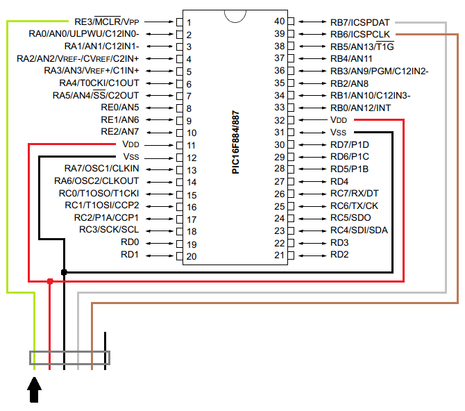
You will need to create another programmer from the circuit diagram below.
Some reason the software I use for my website design crashes when I post the picture of the code, I could do it all in coding but it will save scrolling through the ever increasing program, instead you can follow either of the links to the picture - Program Picture or the - Program Text.
You will need to remove everything on the previous breadboard and start again, here is another visual representation of my circuit on a breadboard. Note that there should be 4k7 pull-down resistors on the row pins and a 50 ohm resistor between the LCD's back light and it's supply.
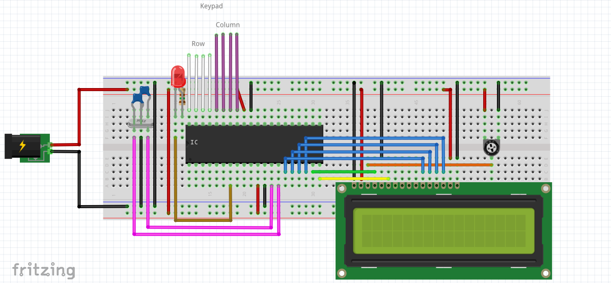
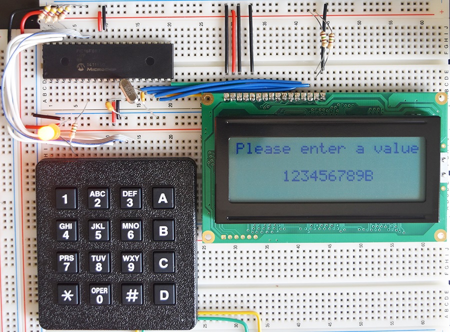
Below is my circuit on the breadboard
Now we have proved that we can quite easily upgrade chip without changing the program too much, it is now time to learn some more of what the chip can do, such as reading analogue. The next project will save a couple of analogue values such as that of what a data-logger would do.
Hello, if you have enjoyed reading this project, have taken an interest in another or want me to progress one further then please consider donating or even sponsoring a small amount every month, for more information on why you may like to help me out then follow the sponsor link to the left. Otherwise you can donate any amount with the link below, thank you!