The 18 Series Microcontroller
This is the start of a series of chapters explaining and showing how to use the peripherals on the 18 series of microcontrollers by Microchip. I intend to write these with the aim of those with little programming knowledge, a basic understanding in electronics is a must and so is an understanding of both binary and hexadecimal. I would first recommend reading through the 16 series chapters I have written just incase I don't manage to cover every aspect of programming and microcontroller architecture.
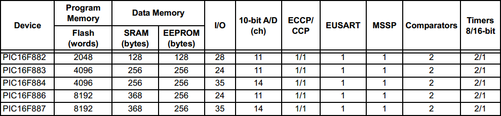
So why use the 18 series over the 16 series. Here are some attributes taken from a common set of chips from the 16 series range, one I used a lot was the 16F887.
Here is the same kind of information but taken from the datasheet of the 18 series.
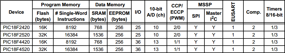
As you can see there is a huge upgrade in both the flash memory and the SRAM. The flash memory is the program memory and each 2 bytes represents one instruction, so 16k of flash equates to 8k of instructions. The SRAM is the temporary memory storage which is used in variables, 256 bytes is very little for most applications, the number of inputs and outputs are essentially the same. An important upgrade here are the number of timers and their size, as you'll read on timers are a very important part of the microcontroller for precise timing intervals.
For me the reason to upgrade chip is not so much the memory but rather the running speed or more precisely the clock frequency. The clock frequency is the speed at which a microcontroller can process instructions, this clock frequency is either controlled externally via a crystal or internally via a resonator, a combination of frequencies can be achieve through the configuration of the chip. The 16F887 had a maximum internal frequency of 8MHz and required an external 20MHz crystal to run at it's full potential, this took up two I/O (input / output) pins. The beauty of the 18 series is that they can internally increase their internal clock frequency up to 4 times via a PLL ( Phase Locked Loop). The basic 18 series will run 40MHz external and potentially 32MHz internal, some of the 18 series will run 64MHz internal which is the maximum speed of the chip negating the existence of an external crystal. For the Microchip range of microcontrollers the instruction speed is a quarter of the clock frequency, so 4MHz clock would be 1MIPS (1 Million Instructions Per Second).
The price of the 18 series is very much the same as the 16 series but I would highly recommend starting with the 16 series due to the architecture and the instruction set. The number of instructions for the 16 series is 35 which are quite simple but do take some practice to remember whereas the 18 series has a total of 75 instructions which can be quite daunting to learn when beginning. The 18 series caries these extra instructions to actually reduce the program memory since these new instructions can skip processes that we required due to the limitation of the 16 series. The problem is that introducing more instructions opens up more ways of writing programs and takes a lot more time to learn all of the short cuts.
Architecture
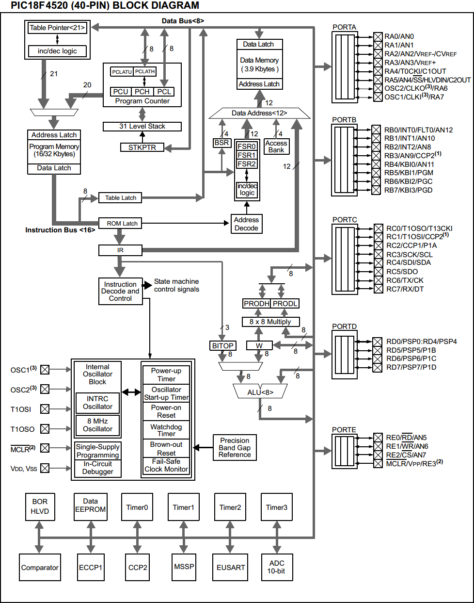
The first thing to discuss is the architecture of the 18 series, more notably the 18F4520 which I will choose for the majority of these chapters. It may be worth reading the first few chapters numerous times in order to understand how a microcontroller works, those new may find these next few sections a little difficult to follow.
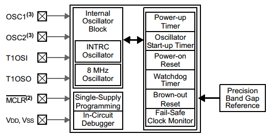
For every datasheet you will get a diagram such as the one below, this tells us how each section of the microcontroller is linked and how many data lines are used to link the data.
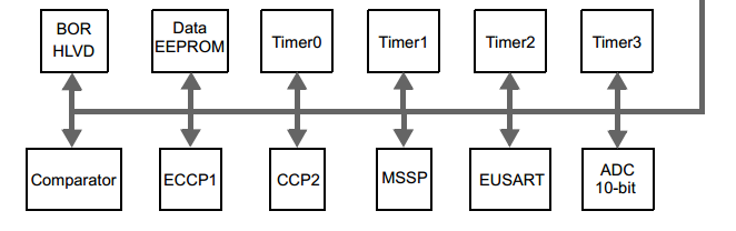
Ports and Peripherals
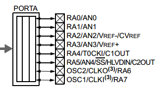
Just a quick explanation of the ports. These are the inputs and outputs of the chip, they all have special abilities and must be configured to run that ability. The abilities may range from digital inputs, digital outputs, serial, SPI, ADC and many more. The ports are controlled by a set of latches which are a form of switch, these switches control how the data is linked to the port and how the port must react to that data.
Attached to the ports are the peripherals, these are all of the special modules for example reading analogue. There's no real need to explain these further as each chapter will be concentrating on each one of these peripherals.
Memory and Program Counter
The main part in a microcontroller is it's memory and program counter, as you will later realise a microcontroller is mostly a large stack of memory and all we're doing is moving it around.
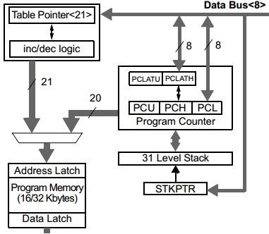
The memory of which is stored in "Program Memory" is a large list of our instructions, the program we have written. A latch is like a set of switches, when they are thrown a certain position they move to a location in the list that is the program memory, the data latch is then the output of that program memory, ie what was stored there, that being our instruction.
The program counter tells us where we are in the program, so for example if it contains say the number 100 then it will be at line 100 in the program memory and take the information from there, when the chip has done with that instruction it will increment the program counter to 101 to take us to the next instruction to read. The program counter tells the address latch where to point.
The table pointer is like a secondary program counter except this lets us read and write sections of the program memory without affecting where we are in the main program, ie the program counter.
The stack is a total of 31 memory locations, if the instruction calls for us to jump to a different part of the program by changing the program counter then the original location value is saved, if we call another then we jump to another stack. When the program returns it reads the previous stack and loads that to the program counter making us jump back to where we left off.
The last part "STKPTR" is just something to tell us when we have exceeded our stack level, this is often not needed.
Here is an example of the program memory and the stack level.
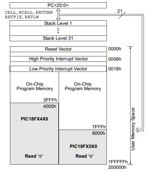
All in this diagram is memory.
The "PC" which is the program counter contains a number, this is the memory line number, it can count to a maximum of 7FFFh which is our memory limit of 32kbyte. You will notice that all memory locations will be stated in hexadecimal.
The next are our 31 levels of stack, we have an instruction called "call" which is a subroutine. The purpose of a subroutine is to jump to another part of program to execute something common to the program, such as a delay. It saves much more memory by temporarily jumping to a delay rather than writing the delay each time. After the subroutine has been complete it will "return" from where it left off in the program.
When a call is issued the current program counter value is saved in the first stack level, the program counter then changes to where it has been called to and starts reading that program. When it reaches the "return" command it loads the stack back into the program counter to return from where it was called.
A total of 31 subroutines can be issued, each return loads the previous stack.
The start location of our program memory is 0000h and spans to 7FFFh for this particular chip. The program counter will start from zero on reset however we normally start writing our program from 0020h. The parts of the program before this are called the "Interrupt Vectors", when an interrupt is called it acts like a call and the program counter will load this location, this will be explained in a later chapter.
Data Memory and SRAM
The data memory is one of the most accessed parts of the chip, it controls all the peripherals and can store all our variables. It must be noted that all of the data memory is in fact SRAM (Static Random Access Memory) and all of it is volatile, it looses all it's memory when the power is lost. I must also note the big difference with program memory and SRAM is their write times, since program memory is flash it can take around 2ms to complete, thousands of instruction cycles whereas the SRAM takes only one instruction cycle. Flash is permanent but has a finite life whereas SRAM is volatile but has an unlimited number of write cycles.
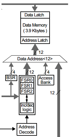
Taken from the block diagram is this part that deals with the SRAM.
The SRAM is broken into two categories; GPR (General Purpose Register) and SFR (Special File Register).
The general purpose registers are those which can contain our variables, these are the randomly accessible slots of memory that we can read from or write to.
The special function registers are those associated with the chips peripherals, they can still be written and read. The purpose is that they contain all the chips settings and tell what data is to be sent out the pins. So for example one memory location will tell eight pins whether they are inputs or outputs and another location will send data out that pin or can be used to read the data coming in from that pin. All SRAM memory locations are known as registers as they contain a registry of information.
These series of chips contain a total of 16 memory stacks similar to how the program memory is laid out. Each stack has a total of 256 bytes, each stack has to be selected separately in order to access the information inside of it. For the data memory each stack is known as a "Bank". The "BSR" (Bank Select Register) is a 4-bit address telling us which bank we want to select, this combined with the 8-bit file register address is placed into our address latch. This points to a specific register in which data can be written to or read from.
Here is an example of how the memory is laid out, the BSF register points to our specific bank and the data from the opcode will point to our specific register in that bank. An opcode is the same as an instruction or command. A particular instruction which only deals with the BSR register is used to load it with a specific value, since each file register is 8-bit the MSN (Most Significant Nibble (the top 4 bits)) are ignored in this command since only the LSN (Least significant Nibble (lower 4-bits)) are used. The opcode instruction will be directing a certain value of data into the data memory addressing register to point it to which location we want to select.
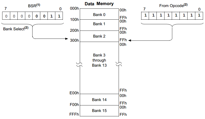
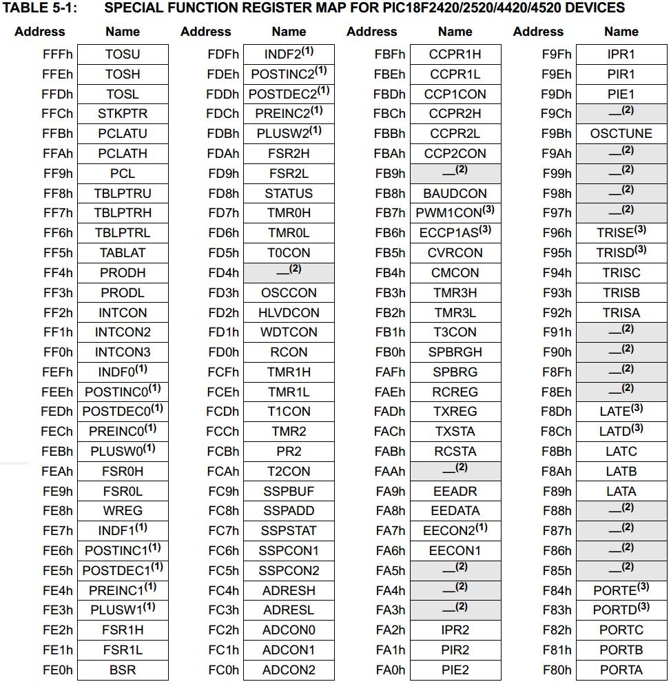
For my particular chip banks 0 through 5 are our general purpose registers, that means there is a 256 x 6 = 1536 bytes available to write to. Bank 15 is our special function register that controls the settings, only 128 bytes are used, all other banks are not used. Here is an example of the second half of bank. So for example If I were to write 0Fh to our BSF and write FFh to 92h we would be setting all of the bits in the TRISA register which controls what pins of port A are inputs or outputs, in this case all to inputs.
This brings me to one more point, direct and indirect addressing. Direct addressing is what I explained earlier by selecting a bank and then writing a value directly to that bank. Indirect addressing is ignoring the BSF register and writing directly to the FSR registers, the FSR registers come in pairs allowing a 16-bit address to be written to them, or rather a 12-bit address. So for example I could write 0Fh to FSR0H and 92h to FSR0L in order for the contents of TRISA to be placed into INDF0. Data can be written or read from INDF0 register which is the same as writing or reading the TRISA register. As you will find out later indirect addressing is much faster for certain applications as we can increment the FSR to jump registers.
ALU
The ALU (Arithmetic Logic Unit) is the heart of any microcontroller as this can add and subtract two binary values. The "W" is our working register which we use a lot, this register holds the data we want to move around. Back in the last section I wanted to plant a number in the BSF, the working register would be first loaded with a value and then the working register transfers it to the BSF, it works much like a bucket.
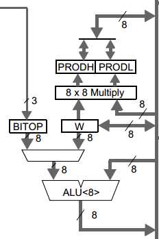
A special feature of the 18 series is the addition of a multiplication module which can multiply together two 8-bit values in one instruction cycle instead of requiring almost 70 to achieve the same thing without this module. The result will be a 16-bit product which is stored in the SFR's PRODH and PRODL.
The BITOP register is just some instructional data from the command that was initiated, it is not a physical register and is no concern to us.
Special Functions
The special functions are the configuration settings when programming the chip, these can however be changed while the chip is running if necessary. The main thing to set is the clock source and it's frequency, there are other important things such as the power-up timer which allows the supply voltage to stabilise before it starts. All of the others will be explained in the next chapter.
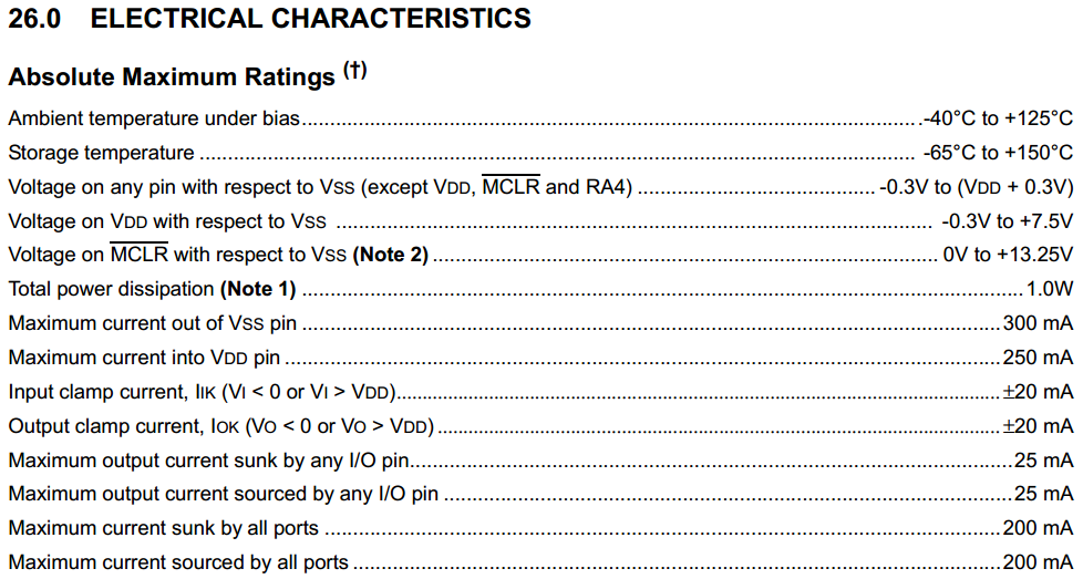
Electrical Characteristics
The last thing in this chapter is the electrical characteristics, if you're upgrading from the 16 series then there is very little difference. The supply voltage is a little more robust allowing it to take an extra volt, now 7.5V, of course you still should run a maximum of about 5.5V. The power dissipation is a little higher but this is to be expected with a higher clock frequency. One thing people look for is the current capability of the pins and most make a mistake of overloading the chip trying to directly run LED matrices, speakers and motors.
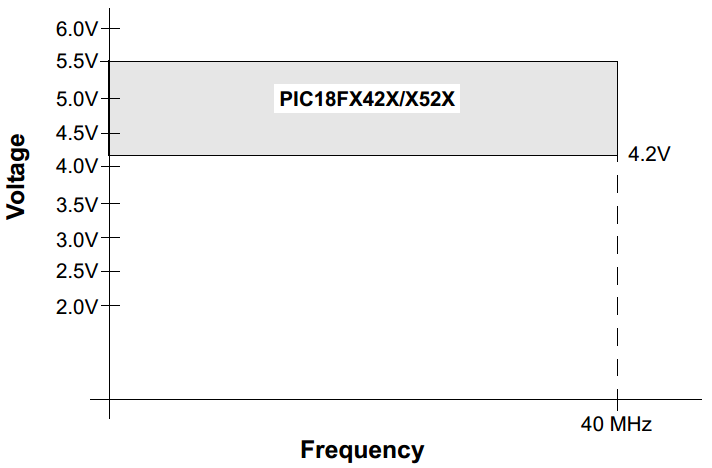
Another aspect to be careful of is the operating frequency with regard to the operating voltage. There are many devices out there that run a maximum voltage of 3.3V such as SD cards but to run a high frequency you can't simply run the microcontroller at these voltages. Compared to the standard 16 series this microcontroller must run on a minimum of 4.2V across the whole frequency range, there is a low frequency option that will run down to 2V at 4MHz. For most applications I need the highest frequency possible so I have to opt for 5V, quite simply a few resistors are required between lower voltage devices.
That's a quick overview of the 18 series microcontroller and what each part does in it's architecture. It's worth being familiar how the memory is organised as all the microcontroller does is move data around. The next chapter is about how to program the chip, the software and hardware that is required. I will also explain the configuration and the special features, I will provide a simple program to test the microcontroller.
Hello, if you have enjoyed reading this project, have taken an interest in another or want me to progress one further then please consider donating or even sponsoring a small amount every month, for more information on why you may like to help me out then follow the sponsor link to the left. Otherwise you can donate any amount with the link below, thank you!