18 Series - Chapter 13 - Serial SPI
Probably one of the most important peripherals on a microcontroller will be the use of SPI serial. The difference between SPI and USART for example is that SPI is synchronised which allows a much higher frequency to be used since a clock signal does not need to be accurate.
What I use SPI for the most is external memory chips and displays, so for this chapter I will be showing communication to the AT25SF161 Flash memory chip. I will also be explaining and demonstrating a process known as "bit banging". So firstly how does SPI work?
Taken from one of the microchip datasheets is the diagram shown below which shows how the SPI links to other devices.
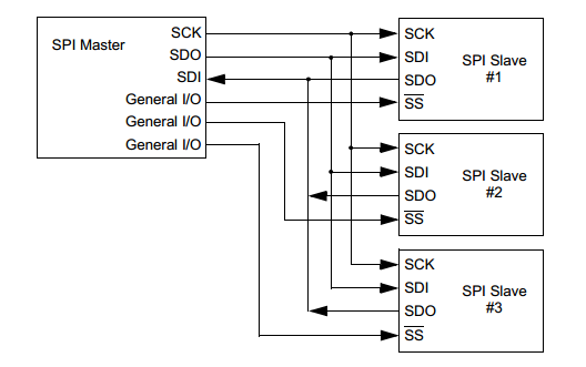
SCK - This is a clock source provided by the master chip, this allows a precise timing of the data to be sent.
SDO - This is the data output line which will be tied to an input line on the other device.
SDI - The input line which is taken from the output line on another device.
SS / CS - This is known as the chip select, this is used by the master to instruct which devices it wants to communicate with, also known as the slave.
So in basics all of the data lines are tied together, data will only be sent or received when the chip is selected.
In general SPI will only send 8-bits at a time, it is common to find 10 and 16 bits variants. SPI is not tied down to a specific data length, it can actually continue without a single pause, it will most commonly be in multiples of 8-bits however. The master chip will raise it's clock signal and then pull a chip select to logic 0 on the device it wishes to communicate with. The data it wants to send is setup on the data line, when the clock signal drops the slave device knows to accept this bit, when the clock is risen the master device also reads the outgoing data from the slave device. This continues until 8-bits have been sent and received. The great attribute with SPI is that data is sent and received simultaneously which is known as "full duplex" mode.
Below is a screen shot of the communication between my master chip and the slave flash memory chip.

The purple trace is the clock, the yellow is the data from the Flash chip and the blue is the data going to the flash chip.
In general the data out will be ready and the clock signal dropping will tell the memory chip to accept this data. In this trace you can see that the data out will drop the same time as the clock, in fact there is a slight propagation delay between the data dropping to the clock signal.
The data out direction is MSB first, so the data is 00000101b which is a special command to the memory chip.
Before I explain how to setup the microcontroller it is wise to learn how the memory chip works first, I will be using what is known as the AT25SF161 which is a 16Mbit flash memory chip. There are other chips out there such as EEPROM (I don't recommend), FRAM (non-volatile like EEPROM but super fast, low storage area), SRAM (volatile RAM, super fast write and large storage area) and then there is of course Flash (Moderate write time, huge capacity).
Taken from the datasheet is this pinout diagram.
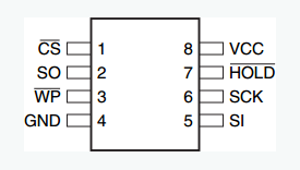
CS - The chip select, this is to be pulled high when dormant, pulled low will select the chip.
SO - Serial out.
WP - Write protect, leave pulled high to enable us to write.
GND - Ground, pull to 0V.
SI - Serial in.
SCK - Clock signal.
HOLD - A hold is used to allow us to pause the chip while we select a different device to communicate with, a hold cannot initiate half way through an 8-bit sequence, pull high for normal operation.
VCC - Voltage common, normally these chips will be 3.3V.
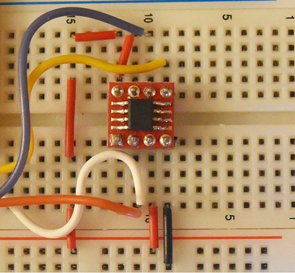
Most commonly these chips will come in the SOIC package so it is a must to get an adapter if working from a breadboard, I have migrated to surface mount for most of my circuit boards since through hole requires more time to drill the holes. Here is an example of the chip on my breadboard.
The first thing we want to do is erase the chip, it is possible to erase sections but a full chip erase is easier to explain for now. The first thing to find is the datasheet command set, a partial extract is shown below.
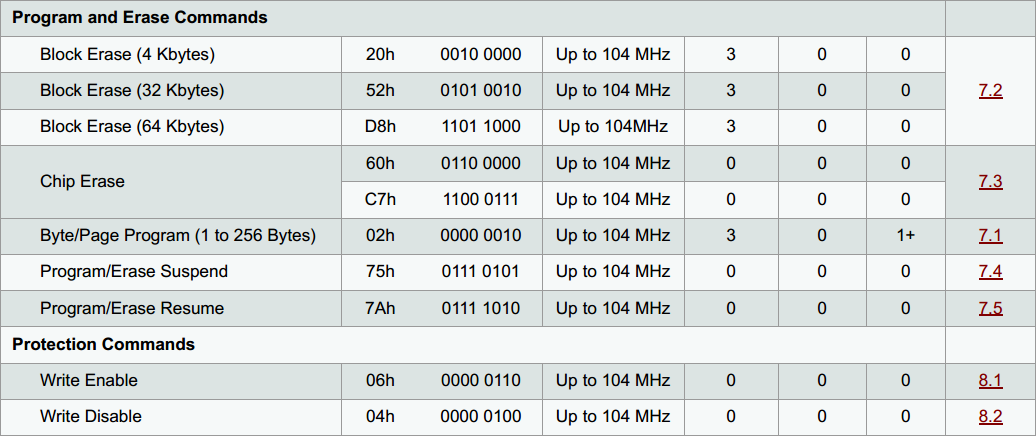
A chip erase can use one of two commands, I normally choose 0x60 but it really does not matter. Now an erase is actually a write to the data storage in which an erase will actually set every single bit high. So before a chip erase the command 0x06 has to be sent in order to enable us to write, it is also known as the write latch. A thing to note with the write latch is that when the chip has written some data or used an erase the latch will open, the command has to be sent again if further data needs to be written.
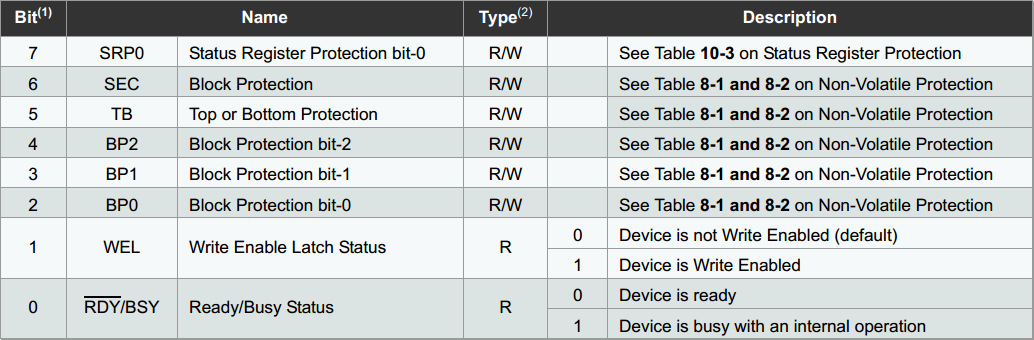
When the chip has been instructed to do a full chip erase it will accept no further commands except to check it's status, de-asserting the chip will not affect the erase process and neither would it in the case of a write, it must be noted that de-asserting the chip will actually start the erase / write procedure. The erase will take around 15ms to complete for this particular chip so it is necessary to keep asking the chip whether it has finished or not. Quite simply we must send the command 0x05 in order for the status register 1 to be read.
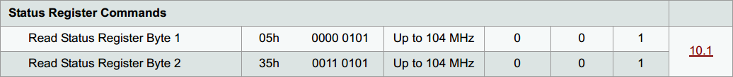
An additional dummy byte has to be sent in which the following data will be sent back, the only bit of concern to use is the read/busy bit, bit-0. Straight after setting the chip to erase the status register will say the chip is busy for around 15ms, the command is continuously sent until the register becomes ready.
A command can only be read when the chip has been selected, in order to select a new command the chip must be deselected and then selected again to send the new command. For the read status command it only has to be sent once, all of the data sent there after will not be read but data will be received showing the status, the dummy data is continuously sent until the desired status is met. So for example here is an oscilloscope trace of the master chip sending the command 0x05 to the memory chip, a dummy byte sent and the status data received.

The data received in this instance is 00000011b which tells us that the write latch is enabled and the chip is busy.
Once the erase has complete the write latch will drop.
We check the busy bit, if not ready then another dummy byte is sent until the chip is ready. The dummy data in this instance is the same as the data I received, this is how my program has been written, the dummy byte can be anything as it is ignored.
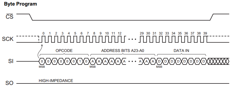
Once the chip has been erased it can be written to. Firstly the chip must be de-asserted and then reasserted in order to send a new command. To write to the chip the write latch has to be enabled, so the command 0x06 is sent, the chip de-asserted and the reasserted in order to send the write command afterwards. The command 0x02 is sent to initiate a write which allows us to write between and 256 bytes. 256 bytes are known as a page, this size can vary between devices. With a flash chip a whole page has to be erased in order to be written to, pages cannot be crossed when writing to, the previous page has to complete it's write before another is written to.

Once the write command has been sent an address has to follow, a 24-bit address. Each bit in the address will correspond to a byte in the memory, remember though that pages have to be written to in multiples of 256 bytes. So for example address 0x000000, then 0x000100, 0x000200, etc... After the address has been sent up to 256 bytes can be written, any more will cause the pages to roll over and start again. Once the data has been sent the chip is de-asserted to start the write process, the chip reasserted and the status checked until the write is complete.
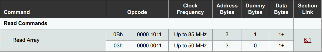
Reading from the chip is much simpler, this time either the command 0x03 or 0x0B has to be sent. The difference is that command 0x0B requires a dummy byte after the address whereas command 0x03 does not. The clock frequency of the 18 series SPI running at 32MHz will be 8MHz, so command 0x03 should be used. The same procedure, command, 24 bit address and then data out. The difference with the read is that it will sequence through the whole of the memory before looping back to the beginning.
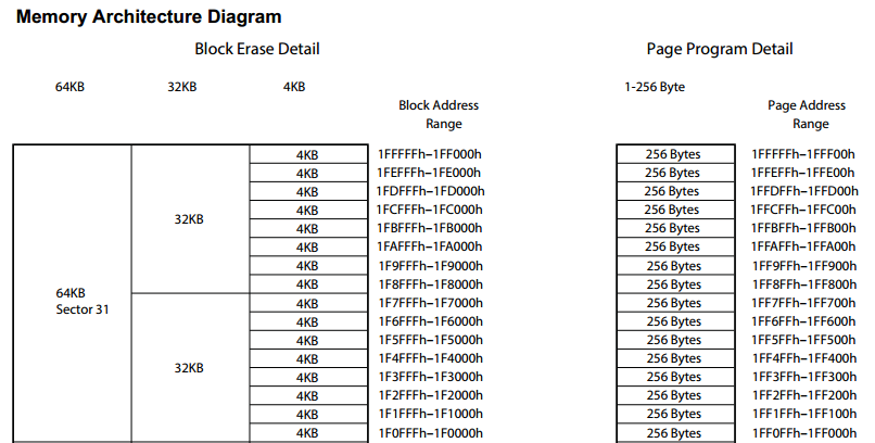
The last thing to discuss with this chip is the memory structure as you may not want a full chip erase, you may want to erase a page or a block instead. This diagram from the datasheet shows how the data is structure, so for example the right shows that a write can only be done in 256 bytes sections. The left part of the diagram shows that blocks can be erased in multiples of 4, 32 and 64 KB.
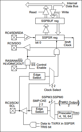
Now we know how the memory chip works it is time to configure the microcontroller. Most, if not all of the 18 series will have a diagram such as that below, taken from the datasheet. As you can see in the diagram there is one main register "SSPSR" which sends the data out as it simultaneously receives data in, it is not directly readable. The data we access is in the "SSPBUF" register which when written to will initiate a send and the data received will be transferred into it. The lower half of the diagram shows the various clock sources that can be used.
The 18 series of microcontroller has many variants in terms of performance, the 18F4520 I have chosen for these chapters is mid-range. If you read on though my website you will notice that some of the high range devices such as the 18F24K40 may have additional registers associated with peripherals and have many more options to choose from. Luckily for this particular chip there are only three main registers which concern us with SPI. The first is the SSPBUF, a buffer register as I explained earlier which contains the data we received. The second register is the SSPSTAT which is the status register.
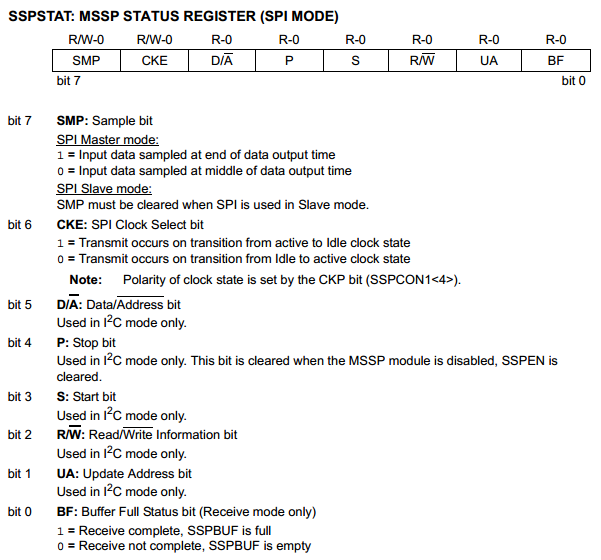
SMP - The sample bit, when the clock is dropped low the data can be read in the middle of this low period or at the end, I have always chosen middle but it really doesn't matter unless the device your communicating with has a slightly different output timing.
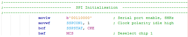
CKE - The clock select bit is generally determined by the clock polarity which I will explain in another register. I always set this bit as zero. Further down the page I will show the difference this bit makes in a transmission.
bits 5 to 1 are used for a particular SPI mode known as I2C which I will not be explaining any further in this chapter.
BF - Buffer full bit is probably the most important bit of this register, this will let us known when data has completed sending and also when data has been received.
The third registers is the SSPCON1 control register.
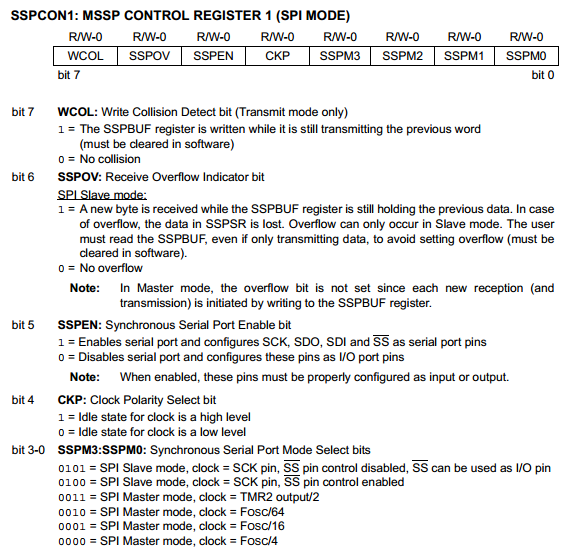
WCOL - A collision occurs when data is loaded to the SSPBUF when the previous transmission has not complete, this would be due to poor program design, in almost all circumstances this bit is not needed.
SSPOV - Even though I will be choosing to run the microcontroller in master mode for this chapter it can also run in slave mode. This bit is used to flag when a second lot of data is received when the previous has not been read.
SSPEN - Serial port enable, if disabled the pins will default to regular I/O's.
CKP - The protocol for SPI transmission is that the idle state for the clock signal is high, a transition to low initiates a start.
SSPM - These bit's choose between master and slave mode and what clock source will be used.
Earlier I spoke about the CKE bit of the SSPSTAT register, here is an example of the bit not set sending a transmission of 0xA8 / 10101000b.

Here is an example of the same data being transmitted. The difference is the way the output data changes, instead of changing on a falling edge it changes on a rising edge. Setting this bit is perfectly good for transmitting data but the microcontroller is unable to receive data from most devices when running in this mode.

The initialisation process is very simple.
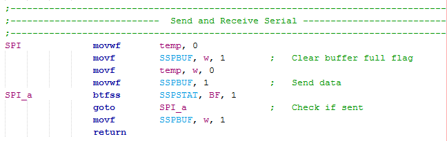
Serial can simply be sent by loading the SSPBUF with some data however the following code ensures there are no overflow errors. The first three lines are actually not needed as long as the buffer full bit is not flagged, they are really just a precaution to ensure an overflow error does not occur.
The first part of this chapter was talking about how to do a full chip erase.
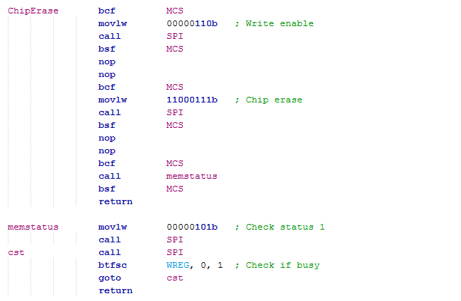
Firstly the chip is selected and the write enable command sent to it, the chip is de-selected in order to allow another command to follow.
The following command is the chip erase, deselecting the chip will initiate the erase sequence.
Finally a sub-program is called which deals with the chips status.
The read status 1 command is sent, dummy data is sent there after until the chip sends back the response to say it is ready. When ready the sub-program is returned and the chip is deselected.
To write to the chip, for this example I will be taking a character from the keypad and saving only one byte.
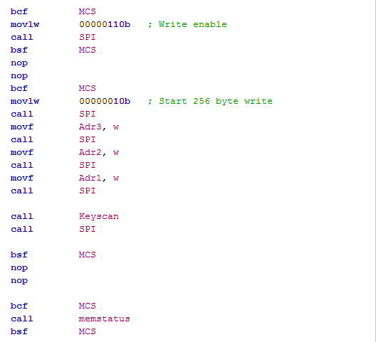
Since the previous action was a chip erase the write enabled latch command needs to be sent again.
The write command is sent along with the address we want to write to, the address being 24-bit in length. This part of the program is commonly a sub-program in which I use three variables with the contents of the address, it is useful when multiple addresses have to be written to.
Afterwards a sub-program is called which reads my keypad and then the data is clocked into the memory chip.
The chip is deselected which initiates the write procedure.
The status is continuously check until the write is complete.
Finally we want to read the data from the chip and send it to a display for example. You may notice that in some of my automotive electronic projects I use these chips a lot to store images to be displayed on LCD's.
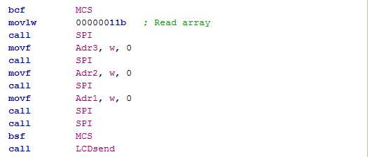
Quite simply the chip is selected, the read command sent followed by a 24-bit address.
A further dummy byte is clocked into the chip while our data is simultaneously read, the data is send to a character LCD on this occasion.
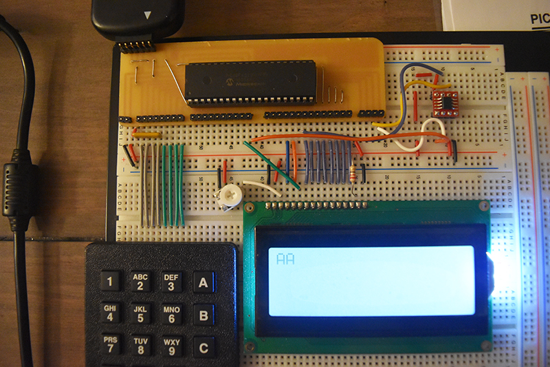
If you have been following these chapters from the beginning then you will know that my current setup is an 18F4520 coupled to a keypad and a character LCD. The following picture is my setup.
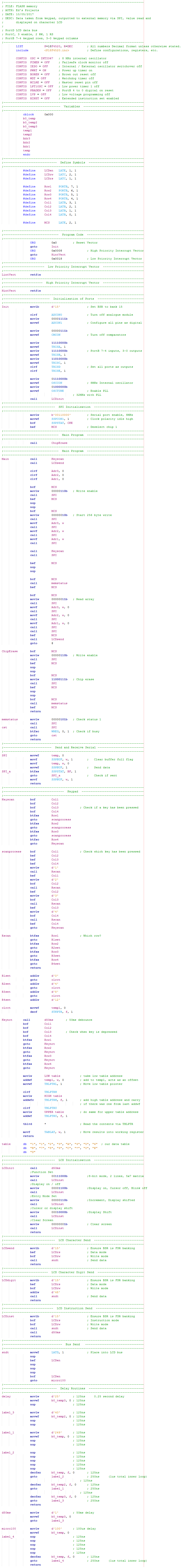
Here is a copy of the program in image form or you can view a text version by following this link.
The last section to talk about is what is known as "bit banging". Most microcontrollers will have an SPI module, some have none and some have many. The fact is that you do not require an SPI module in order to work with SPI, you may notice that in some of my automotive projects that my chip contains one SPI module but I have three separate devices running simultaneously. A problem you my encounter yourself is sending data from a memory chip to a display, the memory chip has a hold function but the display does not, you need some way of replicating SPI. The process of bit banging is relatively simple, you check and send bits, the program is a lot slower than the SPI module but works just as well.
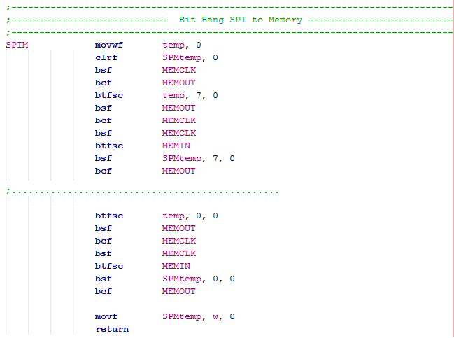
The program is fairly simple. Firstly the working register is loaded with the data we want to send and then it is placed in a temporary register.
The temporary bit is checked to see if it needs to stay as a zero or change to a 1.
The data is clocked.
The data in is checked and loaded to a temporary register.
The whole process is repeated another seven times to cover all 8-bits.
Finally the data that was clocked in is loaded into the working registers before returning the sub-routine.
I think I have pretty much covered all there is with the SPI module, there is of course some interrupts tied to the module but those are straight forward if you read the previous chapter. The next chapter will concentrate on the SD card, how to initialise it, read and write to it.
Hello, if you have enjoyed reading this project, have taken an interest in another or want me to progress one further then please consider donating or even sponsoring a small amount every month, for more information on why you may like to help me out then follow the sponsor link to the left. Otherwise you can donate any amount with the link below, thank you!