18 Series - Chapter 8 - EEPROM, FLASH and the FSR
EEPROM and FLASH and generally considered very similar, they both take similar times to write but EEPROM has a larger write endurance but a shorter lifetime whereas FLASH is quite the opposite. A major difference is that EEPROM is generally written in single bytes whereas flash is always several bytes long, called a page, normally around 32 to 256 bytes. This will be quite a long chapter explaining what each one does and how to read / write them.
EEPROM
EEPROM (Electronically Erasable Programmable Read Only Memory) is quite an old type of non-volatile memory, it is however an upgrade from EPROM which is the old memory chips that had a quartz window in the top that allowed an erase via UV exposure. EEPROM for microcontrollers can only be read and written one byte at a time, there are however EEPROM chips that can be page written as explained in a future chapter.
The reason to use EEPROM is due to it's high number of write cycles and it's memory retention period. What I personally don't like about EEPROM is the fact that it's so slow, taking around 4ms to write one byte. As you will discover later there are far better methods for non-volatile data retention, they are however external.
There are a total of four registers we need to concern with EEPROM.
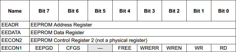
All of the registers are used, EECON2 cannot be read and will be explained later, EECON1 is the only register here that is not clear, below is an extract from the datasheet explaining what it does.
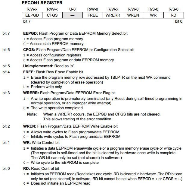
bit-7 - EEPGM - This can be used to select between dealing with the EEPROM or Flash memory (program memory). As you will find out later it is a similar process when writing to Flash.
bit-6 - CFGS - This allows us to select between the Flash / EEPROM or the configuration bits that we set at the very beginning of the program.
bit-4 - FREE - This can be used to erase rows of data in the Flash program memory (64 byte blocks).
bit-3 - WRERR - A write operation error, this is useful as the program can rewrite the data again if this occurs, otherwise the data would have been lost.
bit-2 - WREN - The write enable bit allows data to be written, data can still be read when it is active so it may be best just to leave the bit set. It may be recommended to set this bit at the beginning of the program and leave it unchanged.
bit-1 - WR - When this bit is set it will allow the data to write, when the write has been completed it will clear it. It will take around 2 to 4ms for the write to complete.
bit-0 - RD - When set the data is read wherever the address pointer is pointing to, it is instant for EEPROM and Flash.
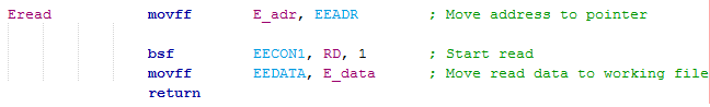
There's not a great deal to talk about with EEPROM so here is the read program. All that is required is the address pointer loaded with the location we want to read from, the read bit is set and the data appears in the EEDATA register. When the read is complete the RD bit will clear, this will only take one instruction cycle.
To write to the EEPROM it takes a little more code.
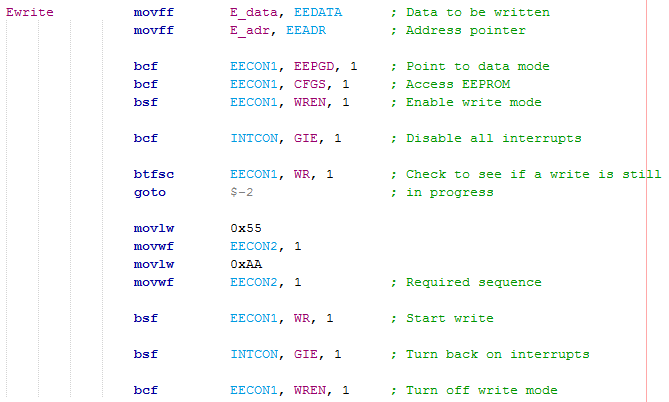
Firstly we have to move our address and data into the correct registers.
The EEPROM module is setup to write to the EEPROM and the write mode is enable (this can be done at the start).
All of the interrupts are disabled, if you have none then leave this line out.
The WR bit is checked to see if a write is still in progress, if not it will skip, if so it will continue to check.
Hex 55 and AA must be sent to EECON2 in order to setup the EEPROM write module.
WR is set to start the write process.
The last two lines can be omitted from the program.
The line that checks the WR bit in the example above uses the "goto $-2" command, this is different to the 16 series since the 18 series uses two 8-bit addresses for one instruction, it concludes that we must jump back 16-bits (2 bytes). This program will just prove that the EEPROM read and write function works.
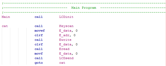
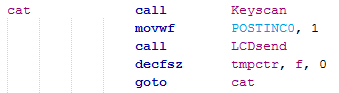
A value is taken from the keypad, saved into an EEPROM address, the data is cleared and then read from the EEPROM address, the value is presented on the LCD.
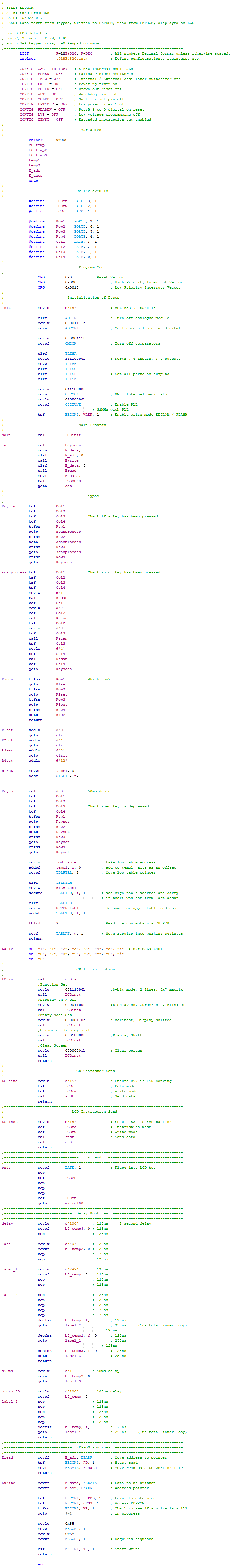
Full Program EEPROM
Here is my full program that reads the keypad, writes the value to EEPROM, reads it from EEPROM and displays the character on the LCD. Here is a copy of the program - Program Text.
FLASH
Flash is a widespread technology used for the storage of data, it is common to find it in microcontrollers, USB storage devices, solid state drives and pretty much everything else that requires mass storage. Flash is comparable to EEPROM as it is an upgrade, the major difference with flash is it's compact size and page write ability. Since most applications require a mass storage such as media it is unlikely that EEPROM even has any applications in the real world anymore especially with another storage type called FRAM which I will discuss in a later chapter.
All flash memory has to be written as a page, a page will generally consist of between 32 to 256 bytes. Even though a page has to be written you can still write a single byte, the difference is that every other byte in the block will be set. Another thing to note is that a page has to be erased before it is written to, this sets all of the bits in the page. When we write to the page all we are doing is clearing bits, so for example writing 11111111b to a memory slot will do nothing but writing something like 10011111b will clear bits 5 and 6.
The first thing to do is work out how the addressing works since this microcontroller can (apparently) write 64 byte pages.
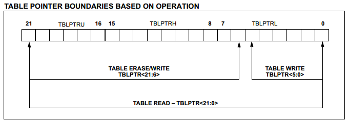
The table pointer addresses are what we use to locate a specific point in the flash memory to either read from it or write to it.
As you can see in this diagram to the left we can read any section of the flash memory.
We can only write a total of 64 bytes (false) and erase pages in multiples of 64 bytes.
I must add that even though the diagram above is for my particular microcontroller it is in fact wrong. I spent some time trying to get the flash write to work but found I could only write 32 bytes. It concludes that this microcontroller can erase a 64 byte block but it can only write 32 byte blocks. The table write pointer is <4:0> instead of <5:0>.
So for example I want to erase a program location such as 0x00AFD0, the part we need to look at is 0xD0 which is 11011111b. Since bits 0 to 5 are ignored it means that 0xD0 would really be read as 11000000b. I could write 0x00AFD0 or 0x00AFC0 as they would both achieve the same thing. Here is an example of the erase program.
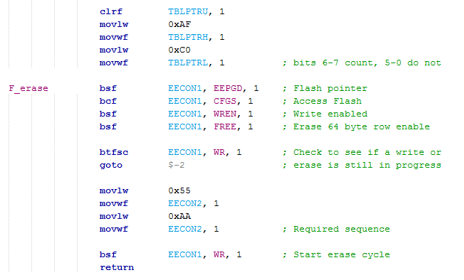
We first load our three registers with the page we want to erase, remember that everything after bit 6 will be erased.
The process is very similar to EEPROM except instead of choosing EEPROM we instead choose to write to flash. The FREE bit is enabled to set the erase condition, this sets all the bits in the page.
Again the write bit is checked to ensure a write is not in process.
The two values 0x55 and 0xAA are sent to setup the write process.
The write bit set to set all the bits / an erase.
Flash Write
The flash write is a little different and requires a few more additional commands. When writing to the flash memory it again is very similar to the erase process but this time we can only write a page of 32 bytes. The difference with writing is that we place our data into the location we want by a table write command, a similar process to writing the EEPROM is used to set the flash memory we have written.
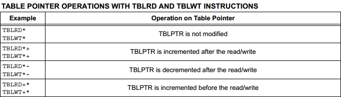
There are a total of eight commands attributed to the table, four of them to read and the other four to write. The main difference is how they deal with the table, so the first two commands just plain read or write whereas the other modify the table pointer.
Since we have to write 32 bytes it makes sense that we increment the pointer after a write (or decrement is some circumstances).
The data does not go straight to the flash using the table write but to a set of holding registers as shown in the diagram below. These holding registers act like ram until we use the flash write procedure like for our EEPROM write.
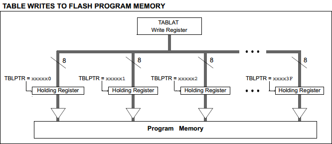
Again the datasheet is wrong since it says the address goes to 0x3F which in fact the actual limit is 0x1F (32 byte not 64 byte).
To write some data to the holding registers we would use a program like below which also introduces us to file select registers and the indirect addressing register. Before a write is issued a block erase has to take place first.
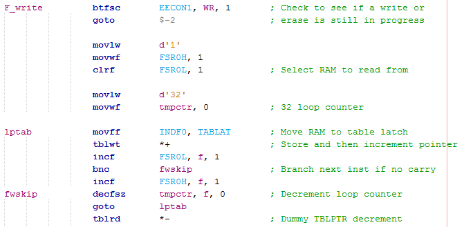
The first step is make sure there is no write in progress.
Next the file select registers are used to point to a location in RAM, this for example will point to bank 1. FSRH is the bank and FSRL is the individual RAM. The contents will then appear in the INDF register. There are a total of three of these modules.
A temporary variable is loaded for a loop counter.
Move the INDF contents to our table latch and then store the information to the holding memory, increment the table pointer afterwards. Increment the FSR's so that the INDF will be updated with the next RAM data. The process will loop a total of 32 times and then branch.
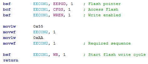
The holding memory is full and now ready to be placed into the Flash, quite simply the same process as to writing EEPROM is used except the EEPGD bit is set to point to the flash memory.
The last part on flash is to prove that the program works, so this program will read the input of the keypad a total of 32 times while displaying the value of the LCD. Once all these values have been input and stored in RAM the program will write the RAM to flash. The LCD will clear and pause for 2 seconds, the flash will be read from program memory and displayed on the LCD. Since the programs are getting pretty large I'm only going to post the main code, a full copy can be found here - Program Text.
Here is an example of the LCD, of course this doesn't really tell you much if the program is working or not.

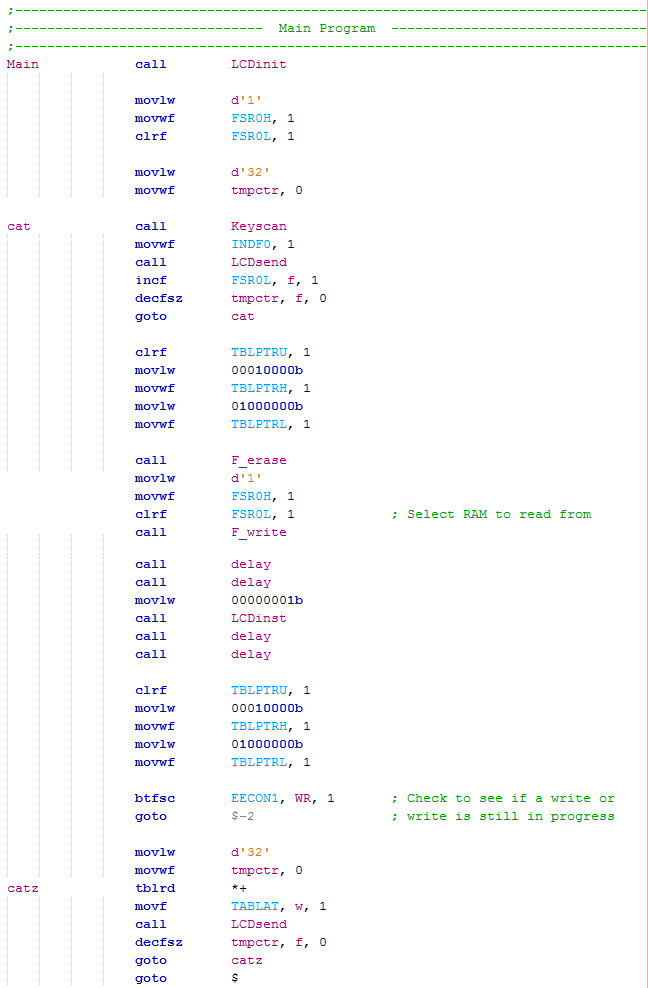
The FSR and INDF
The FSR (File Select Register) is a very important part of the microcontroller programming as we can use it to quickly read and write RAM locations. When something is referred to as "indirect addressing" this is exactly what the FSR and INDF are for. Direct addressing is reading a RAM location directly whereas indirect addressing is loading a set of pointing addresses to find the value in a particular RAM location and the microcontroller placing the result in a specific register. Using the table pointer is another example of indirect addressing.
Here is an example of all three sets of FSR's and INDF's found in the special function registers (FSR's).
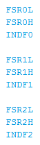
Here is an extract from the datasheet that does a good job of explaining what the FSR's do, the command in the example adds the contents of the working file to the INDF register, due to the FSR pointers the data will be placed in location 0xECC in the RAM.
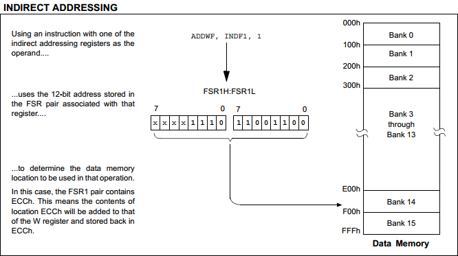
I used an example in the flash write program, this for example loads the INDF0 register with a value from the keypad, the FSR is incremented ready for the next keypad entry to be placed in the INDF.
The 18 series has some additional abilities with regards to the file selecting registers, for example FSR0 has the following file registers attributed to it, likewise 1 and 2 have the same.
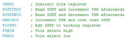
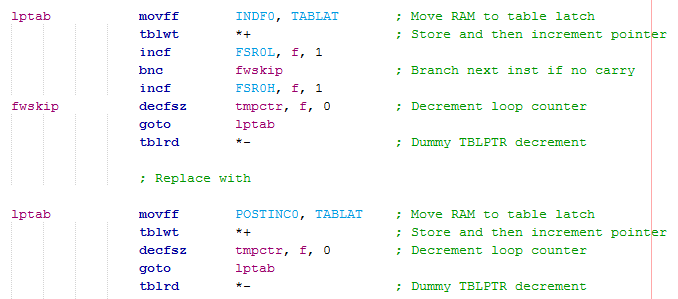
So for example with the above registers I don't have to use incrementing instructions which saves on memory. The previous piece of program that placed the keypad data into the RAM can now be replaced with the following.
Likewise part of the Flash write can be replaced such as in the example below. The beauty of using these registers is the lack of using the increment instruction and checking to see if we need to increment the higher FSR from a carry.
Since I have made these modifications to the program here is an updated copy - Program Text.
This chapter has been a relatively important one as it has shown us how to deal with both types of non-volatile memory storage. EEPROM is ok for single byte write operations but flash is faster, larger and just simply the preferred method for storing data. It must be noted however that EEPROM will have between 10 to 100 times more write capabilities, care must be taken how often flash is written, normally it such things like hardware settings that are set on the rare occasion. The next chapter will discuss the program counter and the stack, it will be a short chapter.
Hello, if you have enjoyed reading this project, have taken an interest in another or want me to progress one further then please consider donating or even sponsoring a small amount every month, for more information on why you may like to help me out then follow the sponsor link to the left. Otherwise you can donate any amount with the link below, thank you!