Microcontrollers 14 - Synchronous Serial Bit Banging - EEPROM
For the past few projects I have used EEPROM to store information, I have needed to be careful when I chose to write it since it takes around 5ms to write each byte, this is very slow. The EEPROM is also very limited in size, at a mere 256 bytes, however this will still take over a second to write. The alternative is to use external EEPROM as it can run at a far higher frequency along with a much larger storage area. Care needs to be taken when choosing an EEPROM chip as they will either run on synchronous serial, SPI or I2C. Normally when it doesn't specify what serial we are dealing with then you can automatically assume that it's synchronous, it will only have two data pins.
I have chosen to go with an ATMEL EEPROM chip - part AT88SC12816C-PU.
It will hold a maximum of 128 kbit and run at a speed of 1MHz, since we are using synchronous it means I can run it at any speed I want up to 1MHz. These chips are also what is used in credit cards, the datasheet will show the varieties. All EEPROM does however take around 5 to 10ms to complete a write, the difference with these external chips is that they can write a page in 5ms, for this chip a page is 128 byte. The read is however instantaneous and will run all the way up to the 1MHz specified by the datasheet. You will notice that this chip closely resembles the I2C protocol as mentioned in a future chapter, however for this chapter I will start from scratch.
There is one thing that must be clear with EEPROM, it has a limited write life that could be destroyed in less than 10 minutes if not correctly used. The write endurance is 100,000 cycles, with a write time of 5ms this could be only 500 seconds worth of usage. The main thing with EEPROM is to write pages which stores more data with less write cycles. EEPROM tends to be written only once such as that for a car ECU or some other type of embedded application, to use it for temporary data storage is a bad design, FRAM would be a better alternative as explained in the SPI chapter.
When a chip is defined as using synchronous serial and not SPI or I2C it will normally mean it's got an unusual protocol. This chip isn't too bad with regard to protocol, it would however be difficult to use the serial module so I will be using a method known as "bit banging", it refers to using a program to read or write serial and not a specialised register to do the work for us. Before all of this we need to know how the data is to be transmitted and what kind of delays need to be implemented. To find these delays there should be a section in the datasheet such as this below, the minimum delays are 200ns or less which is also the speed of an instruction cycle, not many delays are needed but it should be noted that the clock frequency shouldn't exceed 1MHz, or a 1us period.
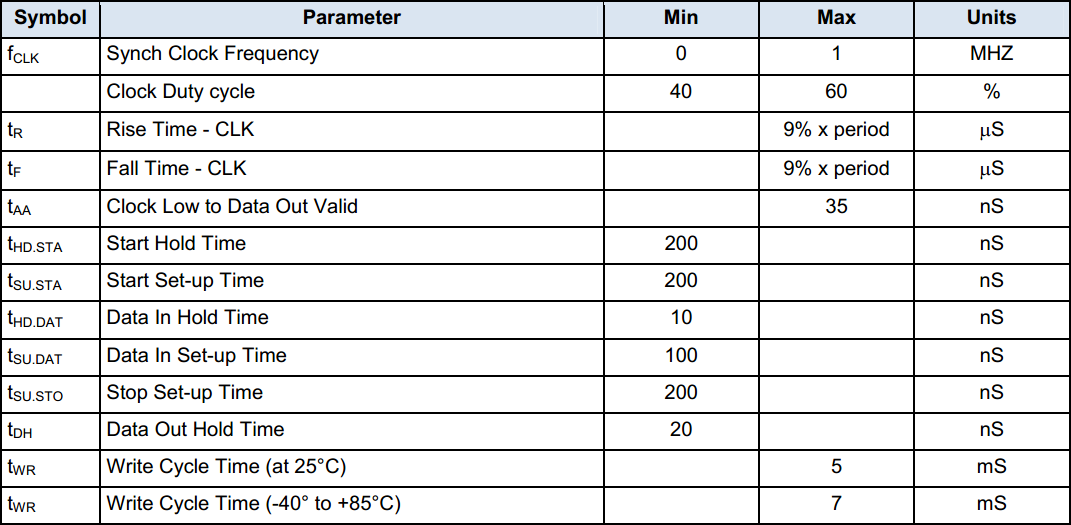
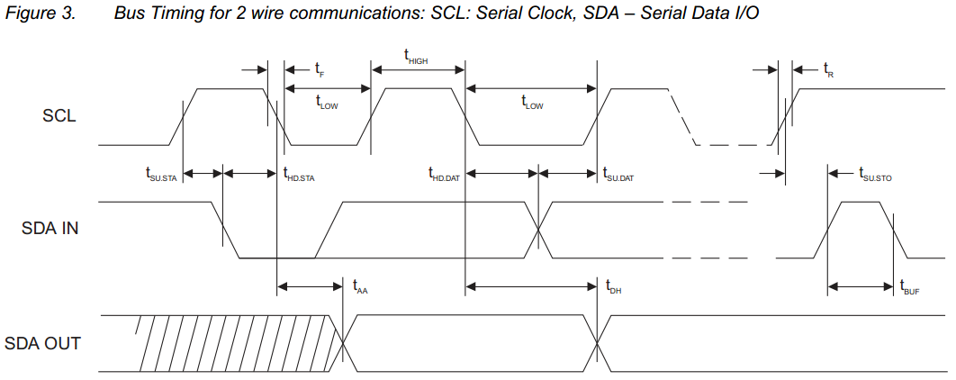
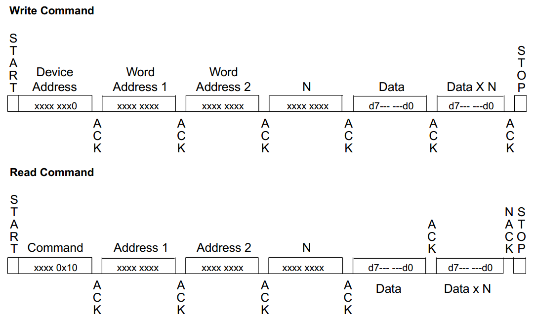
Below is the timing diagram with regard to the table above.
As for the protocols, I chose to take this snippet from the datasheet to save time on re-writing it. The protocols are very much the same for regular synchronous, the only difference is the acknowledge bit which is a little harder to implement using a serial register. The acknowledge bit is used in the I2C protocol however the EEPROM chip is not purely I2C and therefore this register cannot be used.
Here is an example of the timing diagram, it shows that the start condition is set by a change of the data from high to low while the clock pin is high and the stop condition is set by a transition of the data from low to high when the clock pin is high. All data to be sent and received is changed on the low end of the clock cycle otherwise it would create a start or stop condition.
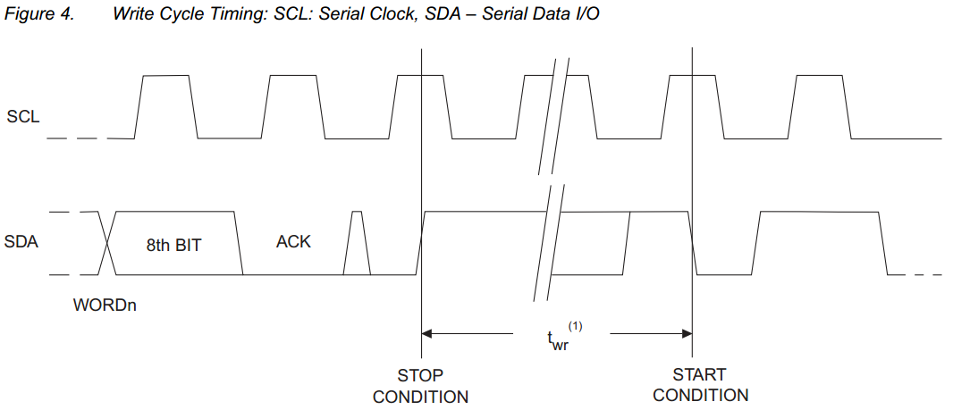
To read or write from / to the EEPROM chip you first have to specify a device address along with a command, the first four nibbles are the address and the last four nibbles are the command. After the command an acknowledge bit is set, it will go to zero when the data has been processed. The next two words are the address we are reading / writing to, the next word will specify how many words we want to read or write and then everything after that is the data, it is ended with a stop command. After the stop command the EEPROM chip will write, another command sequence can be sent to the chip but the acknowledge bit will be set indicating that it is not ready to receive yet more data until the EEPROM has finished writing.
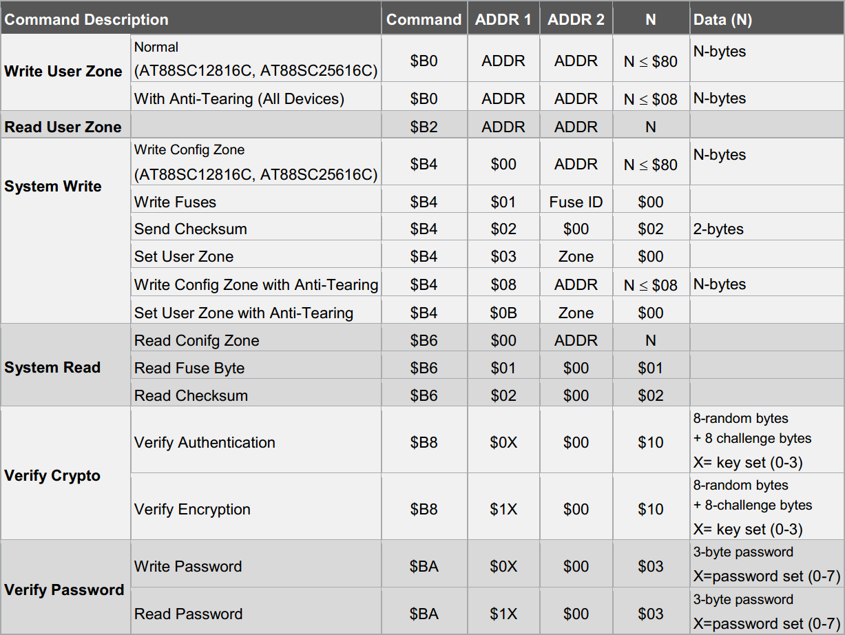
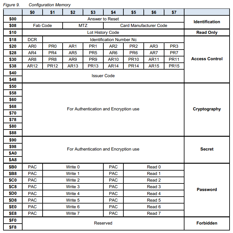
Next are the commands themselves which are presented in the table below. This chip is intended for smart card applications such as for payment machines or even credit cards. These chips can have some of their memory locations locked by a password and have all sorts of configuration settings which can be written. For normal use we only have to access the user read and write zone by using command two and zero, there are also 16 user zones for this chip so the command four has to be used to select which one. The "B" address is defaulted on all of the chips however this can be changed in the contents of the DCR folder as explained later.
The memory structure I'm not going to explain as all I need to use this chip for is to store memory which is in the user zones, the only exception is that I will change the address of the chip in the configuration zone.

Lastly there is one extra protocol the EEPROM chip needs when starting up and that is five clock cycles, that's it, as show in the oscilloscope trace to the left.
Note:
Yellow = Clock
Blue = Data

Here is an example of the start condition, the data line will go high followed by the clock. The data line will fall while the clock is high indicating to the EEPROM chip that a start condition has been set.
The next bit is an example of how data is clocked out, the data transitions only occur while the clock is low.
You will notice about a 0.8V difference between the signals, this is because the EEPROM chip is open drain while the microcontrollers output is push push, a diode has been place in between to stop the microcontroller from pulling the EEPROM chip high when it is pulling it's output low, causing a short.

Here is an example of a data bit, acknowledge bit and the stop bit at the end of a command.
Firstly the data pin has to be turned to an input, the EEPROM chip will pull the data line low if it has received the information. This is the reason for the diode as there could be a short until the output pin has changed to an input pin.
The input pin then changes back to an output which is the cause for the spike, this doesn't matter since the clock is low.
The Clock moves high followed by the data pin, the clock drops while the data pin is high indicating to the EEPROM chip that a stop condition has been set.

Here is an example of the command 04 and the address being sent followed by 03 to indicate user zone write, followed by 0 to indicate user zone zero and then zero to indicate no further data to be sent.
When a write command has been completed it needs to be polled in order for the acknowledge bit to set.
Basically a start instruction needs to be set followed by a word (address and command), the acknowledge bit is checked, if still high it needs to loop again by sending a start bit and the word again.
It will continue to loop until the acknowledge bit goes low, once low a stop bit is sent, the EEPROM chip is now ready for more data.

Here is an example of me sending a write command, the "N" number is set to five as I want to write five bytes of data to the EEPROM chip (look closely, bits 0 and 2 of word 4 are set).
The next five words afterwards are sent, these being the values of 1 to 5.
Once the data has been sent it is finished with an end bit.
Polling then occurs until the acknowledge bit drops to zero, polling may occur for up to 10ms until the EEPROM has been written.

This time the read command has been sent.
Once the commands have been sent the microcontroller pin turns to an input to receive the data from the EEPROM chip.
After each word from the EEPROM the microcontroller turns back to an output to send a zero to indicate an acknowledge.
The very last word is received but this time the acknowledge bit to be sent is high followed by the stop bit.
No polling is necessary as the read command is instant.

Here is a close up of the end of the read command.
The EEPROM chip is known as an open drain which has to be pulled up by an external resistor, the minimum resistor size being 2kohm. Since inputs are capacitive the EEPROM needs to charge the microcontrollers input, a larger resistor would yield a slower rise time and therefore a slower operating speed.
The basic program is as follows in order to read and write to this EEPROM chip, the values to be written are saved in RAM via the FSR, likewise the data to be read is saved also in RAM via the FSR, this part of the program will be changed to suit your application.
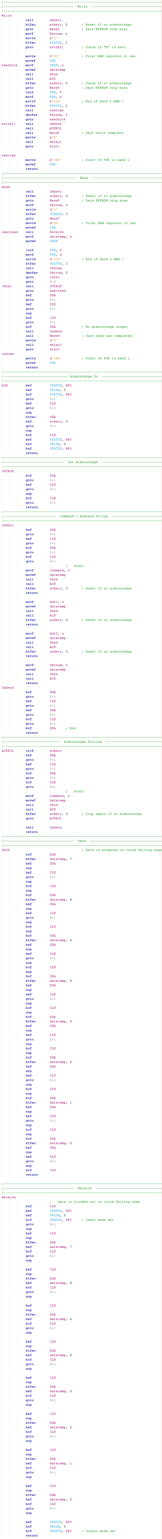
Depending on the circumstances either a read or write command will go to the EEPROM.
Firstly a command string program is called which sends the required information to the EEPROM chip such as the device address, the command, the data address and the quantity of data.
When this program returns it will read the data from the RAM and send it to the EEPROM.
Since the RAM required to do a page write is 128 bytes and a single block of RAM in the microcontroller is only 80 bytes it needs to be spread over two banks. The program will detect when the FSR reaches the end of the writeable RAM causing the FSR to be offset by a different value, this different value is the start address of the RAM in bank one.
The variable "Datnum" is the number of pieces of data to be written to the EEPROM chip, if it is zero then the program will automatically jump to the end and skip all the dealings with the FSR. This variable is also decremented by one each time it sends data, it will only send the specified amount of data ( the "N" number).
Since this is a write command it will call up another program which polls the acknowledge bit, it will only return when the EEPROM has acknowledged and is ready for more data.
The program will then return to the start ready for another read or write.
The read command has a similar process as it must first write to the EEPROM chip specifying device address, command, etc...
The difference this time is that the saved data is placed in the RAM via the FSR, it will again detect the end of the usable RAM in bank zero and offset the FSR so it saves the rest of the data to the RAM in bank one.
Since we are reading we must now send a bit towards the EEPROM chip to acknowledge that it has received the data. At the end of the process the last acknowledge bit must be positive as part of the protocol.
The process finishes with a stop bit and then returns to the start of the program to receive either a read or write command. There is no polling needed with the read as it is instant.
This acknowledge program is for when writing to the EEPROM, if first sets the data pin to an input to read the acknowledge.
The acknowledge bit should be zero, if not then it will load a variable as an indicator that it has not acknowledged the data, when this section of program is returned it will flag an error message on the LCD and set the program back to the start.
The pin is set back to an output and returned.
The out acknowledge is used when reading from the EEPROM, this simply clocks a zero to the EEPROM chip to tell it that it's ready to receive more data.
This is the main program that is used in both the read and write.
It first starts off by creating a start condition for the EEPROM.
A variable called "command" contains the device address and the command, this is sent to a program which bit bangs the serial out to the EEPROM. The acknowledge bit is checked, if unsuccessful the program will return and the program before that will reset back to the start.
Address one is sent.
Address two is sent.
Finally the number of words to be dealt with are sent, the program is then returned to either read or write the data depending on what the command was.
This little section of program is called when all of the data has been processed, it is the stop bit.
Acknowledge polling is only used in a write command.
It sets a start condition and sends a command, if the acknowledge is received then it will call a stop bit and return the program. If it does not receive an acknowledge then the program will continue looping by sending a start bit and command until the acknowledge is met.
This program may loop for as long as 10ms until the EEPROM has finished it's write cycle.
The send string is the bit banging part of the program.
It simply reads each individual bit in a temporary variable, the bit is clocked out to the EEPROM.
The next bit is checked in the variable and the same process happens again.
The program will clock each bit of the temporary variable until all eight bits have been sent.
The program returns from where it was called.
To receive information the data pin is configured to an input.
The pin reads the data received and places all of the individual bits in the temporary variable.
The program is returned from where it was called.
As you can see with the above program the bit banging part is really simple, the more complicated part of the program is dealing with the data.
The previous section of code is just a snippet of my program. With all of the delays I have included in my program it comes to around a speed of 500 kbit/s which is fast enough for most applications, any faster for this application it may not allow enough time for the EEPROM chip to charge the microcontrollers input, again it all depends on capacitance in the circuit.
Here is a link to the - Program
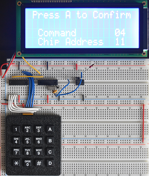
The user can select the command, chip address, the data addresses and the quantity of the data to be read / written.
The data to be sent to the EEPROM for this program are just the numbers one to "X" incrementing by one, this could be any data such as the analogue readings such as in one of the previous chapters.
I chose to use a single chip to control the keypad which sends a serial value to the master chip, the master chip then communicates to the EEPROM chip via serial.
As you can see the circuit is rather simple, since these chips can have an address written into them of between 0 to 15 it means that only two pins are needed to control fifteen chips (All chips will respond to address 11 / B). A thing to note is the capacitance of the circuit as this will reduce the reliable operating speed.
To change the address of the chip you must first access the DCR register, to find this location you must first look at the configuration memory map of the EEPROM device. As you can see the DCR is address $0018, therefore you must first send "00" in address one and then "18" to address two. Since we are only writing data to the DCR byte the "N" number must be set to one.
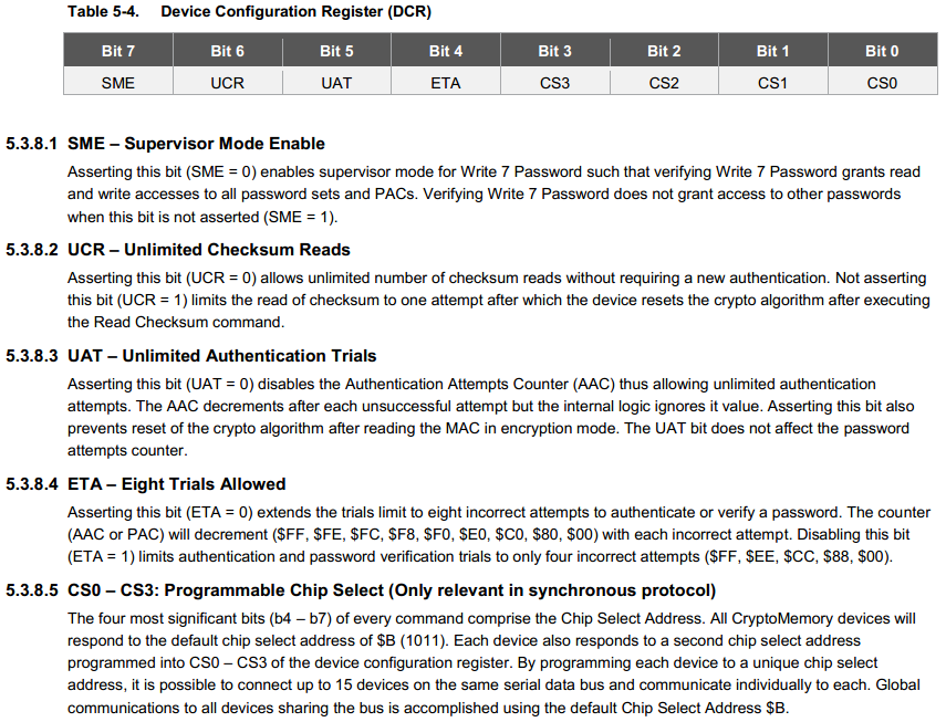
Taking another extract from the datasheet you can see what the bit's in this configuration register need to be set to. Since I don't need a password or any kind of protection on the EEPROM chip the first four bits can be set to zero, the next four bits will determine the chips identity address. Note that 11 or B will respond on all of the chips, therefore you can have a maximum of fifteen independent devices.
I hope you now get how to bit-bang serial, the most work is finding out the command protocol. In one of the future chapters I will discuss the I2C protocol which you will find to be very similar to the protocol for this EEPROM chip. EEPROM is old technology now, it's slow and has a very limited life. The next chapter will discuss FRAM which can be written at high speed but will retain it's memory for decades, it will require the use of SPI.
Hello, if you have enjoyed reading this project, have taken an interest in another or want me to progress one further then please consider donating or even sponsoring a small amount every month, for more information on why you may like to help me out then follow the sponsor link to the left. Otherwise you can donate any amount with the link below, thank you!